Chapter 1
What An FPGA Is
Contrast ASIC geometry with FPGA configuration, then connect concurrent Boolean logic to state that advances at clock edges.
Seven chapters · one circuit from logic to pins
An FPGA gives every logic function, register, and route a physical place where it can operate at the same time.
Begin with Boolean functions and clocked state. Enter the LUT-and-routing fabric. Write Verilog, drive it with a self-checking testbench, inspect its waveform, assign board pins, and carry the circuit through synthesis, place-and-route, bitstream packing, and an iCE40 board.
Each chapter adds one concrete object to the same machine: LUT, flip-flop, toolchain, source hierarchy, counter, constraint, routed configuration, and visible board output.
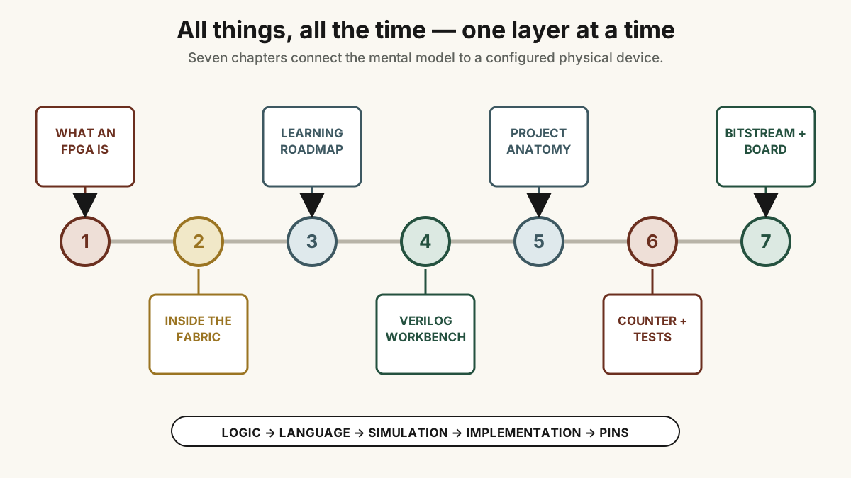
Chapter 1
Contrast ASIC geometry with FPGA configuration, then connect concurrent Boolean logic to state that advances at clock edges.
Chapter 2
Trace a signal through LUTs, flip-flops, local switchboxes, long routes, memories, DSP blocks, clocks, and I/O cells.
Chapter 3
Move from Boolean logic and Logisim into HDL, simulation, board I/O, CMOS depth, and ASIC implementation in a useful order.
Chapter 4
Install Icarus and GTKWave, run the included counter testbench, inspect its VCD waveform, and bring in Verilator for C++ integration.
Chapter 5
Connect source files, module hierarchy, the selected top, the design under test, timed stimulus, executable checks, and board constraints.
Chapter 6
Turn the CD4029B datasheet into executable counter behavior with load, direction, binary/decade modes, wrap, carry, and cascade.
Chapter 7
Use Yosys, nextpnr, IceStorm, and the Alchitry loader to turn Verilog, constraints, and a selected board revision into a visible LED sequence.
Simulation makes behavior executable. The testbench drives inputs, clocks time, checks outputs, and records transitions. Implementation then assigns package pins, maps device resources, routes signals, and analyzes timing. The board turns the configured circuit into a visible physical result.
Analogies open the door; hardware structure carries the lesson. SQL, publish/subscribe, software I/O, an Arduino loop, and reactive programming each illuminate one aspect of HDL. Verilog describes concurrent hardware processes, while statements inside each procedural block still follow the language's ordering rules.
The seven chapters establish the vocabulary that every programmable fabric must answer: logic, state, placement, routing, timing, configuration, I/O, and observation.
That foundation makes the transition to Cartilage productive. Conventional FPGA tools place a design into a vendor fabric; Cartilage explores locally coherent spatial regions, visible routes, and runtime replacement from another architectural direction.