Extract Six Behaviors From The Datasheet
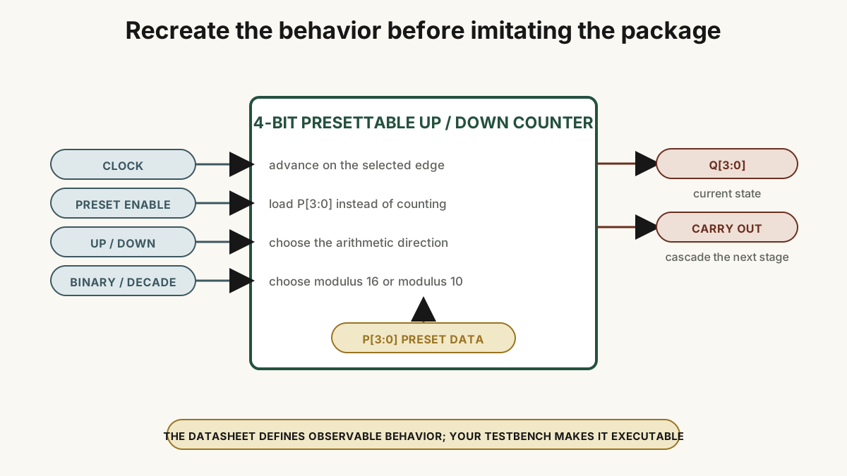
The Texas Instruments datasheet defines the CD4029B as a CMOS presettable up/down counter. Six behaviors shape the Verilog architecture and its tests:
- Four storage stages expose the current state through four buffered outputs.
- One mode control selects binary or BCD-decade counting.
- One direction control selects upward or downward counting.
- An enabled positive clock transition advances the state.
- Preset enable transfers four jam inputs into the stored count.
- An active-low carry output marks the terminal state for cascaded counters when carry-in enables counting.
The control polarities matter. A low CARRY IN enables counting, so the pin also acts as an active-low clock enable. High BINARY/DECADE selects binary; low selects decade. High UP/DOWN selects up; low selects down. High PRESET ENABLE transfers the jam inputs.
Each row maps directly to an input sequence and an expected state, turning the datasheet table into executable design work.
Translate The Preset Path For FPGA Storage
The physical CD4029B transfers jam-input data asynchronously while preset enable stays high. FPGA flip-flops typically provide a clocked data input plus a limited set of asynchronous controls such as reset or set. They do not generally offer an arbitrary four-bit asynchronous data load.
The project therefore keeps two useful forms:
- Datasheet simulation model: represent the asynchronous preset and exact control polarities when a system needs the original pin behavior.
- Portable FPGA implementation: load jam data on the rising edge while retaining binary/decade selection, up/down control, enable, terminal count, carry, and wrap behavior.
The named synchronous load makes the target architecture explicit. This translation shows how an HDL interface can preserve a device’s computational behavior while adopting the storage resources that the FPGA fabric implements efficiently.
Implement Every Mode In One Clocked Counter
The simple counter from chapter 4 supplies the clocked-state skeleton. Mode, direction, enable, jam data, synchronous load, and terminal detection turn it into the full FPGA-portable design:
module cd4029b_counter (
    input  wire       clk,
    input  wire       load,
    input  wire       enable,
    input  wire       binary_mode,
    input  wire       up,
    input  wire [3:0] jam,
    output reg  [3:0] q,
    output wire       carry_out_n
);
    wire [3:0] maximum = binary_mode ? 4'd15 : 4'd9;
    wire terminal = up ? (q == maximum) : (q == 4'd0);

    assign carry_out_n = ~(enable && terminal);

    always @(posedge clk) begin
        if (load) begin
            q <= jam;
        end else if (enable) begin
            if (up)
                q <= terminal ? 4'd0 : q + 1'b1;
            else
                q <= terminal ? maximum : q - 1'b1;
        end
    end
endmodule
The interface presents FPGA-friendly positive logic. enable inverts the physical part’s active-low carry-in or clock-enable function, binary_mode expresses binary selection directly, and load names the rising-edge jam transfer.
Decade-mode operation uses valid BCD states zero through nine. Applications that load ten through fifteen can derive the desired transition behavior from the detailed device logic and encode that policy explicitly.
Run cd4029b_counter.v with cd4029b_counter_tb.v. The accompanying Makefile and README.md place the compile command and expected completion message beside the source.
Turn Every Control Combination Into A Test Vector
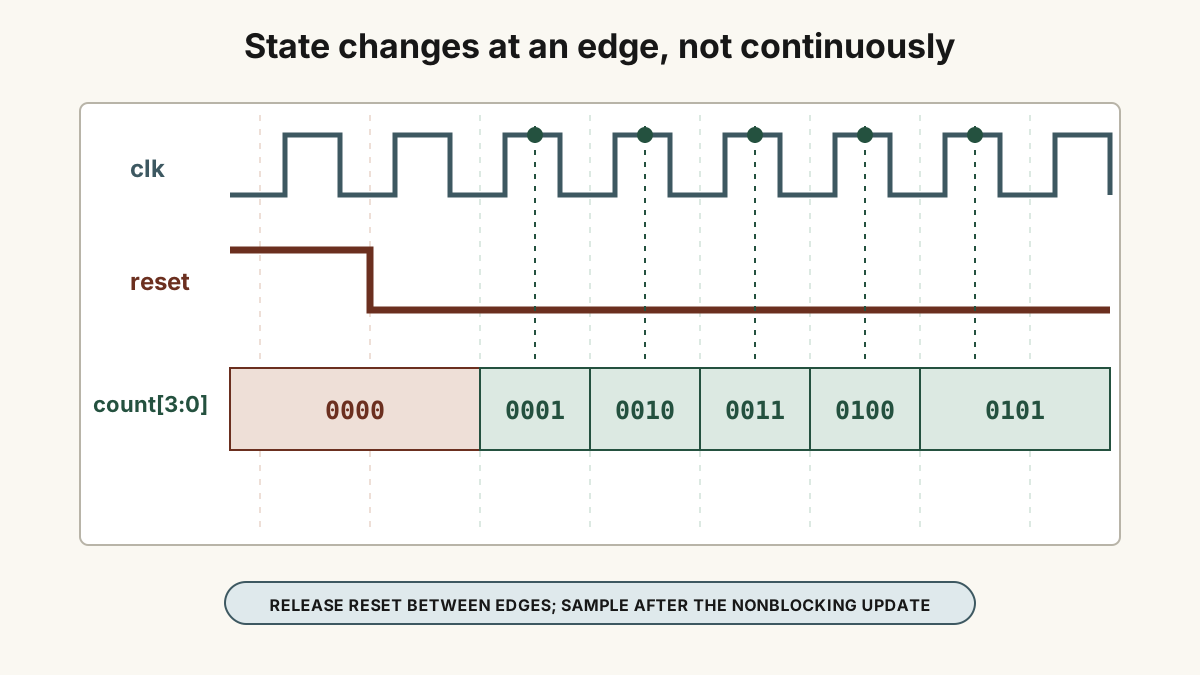
Name the starting state, controls, clock event, and expected result before opening the waveform:
jam=5 and load=1, the next rising edge produces five.enable=0, repeated rising edges preserve the loaded value.A task can remove clock-driving repetition without hiding expectations:
task tick;
    begin
        @(negedge clk);
        @(posedge clk);
        #1;
    end
endtask

task expect_q;
    input [3:0] expected;
    begin
        if (q !== expected)
            $fatal(1, "expected q=%0d, observed q=%0d", expected, q);
    end
endtask
The one-time-unit delay follows directly from simulator scheduling. A nonblocking assignment updates the register after the clock event’s active region, so the task samples after that update. SystemVerilog clocking constructs offer another race-free sampling method.
Make Each Invariant Executable
An assertion converts “this must be true here” into running code. A direct Icarus-compatible testbench can enforce the decade-state invariant with an immediate check and $fatal:
if (binary_mode == 1'b0 && q > 4'd9)
    $fatal(1, "invalid decade state: %0d", q);
SystemVerilog concurrent assertions express temporal relationships such as “an enabled binary up-counter at 15 reaches zero at the next sampled state.” Match the syntax and invocation flags to the selected simulator, then grow the immediate checks into those clocked properties.
Chapter 5 provides the course’s common Verilog language reference. This chapter applies that language directly through executable assertions.
Use Packed Vectors And Unpacked Arrays Deliberately
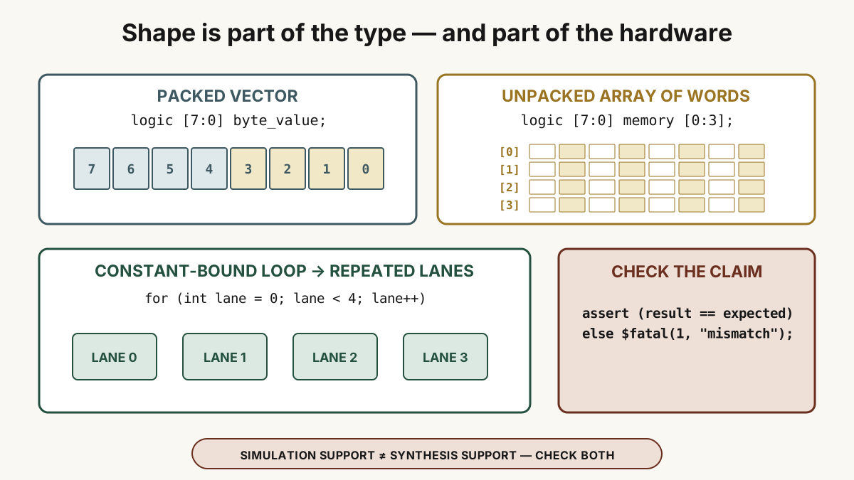
Array punctuation defines the data shape:
logic [7:0] byte_value;       // one packed eight-bit vector
logic [7:0] memory [0:3];    // four unpacked elements, each an eight-bit vector
In the first declaration, byte_value[7] selects one bit. In the second, memory[2] selects one byte and memory[2][7] selects a bit within that byte. The packed range appears before the name; the unpacked range follows it.
Range direction also affects the mapping. [7:0] and [0:7] both contain eight bits, but they assign different left and right indices. State the bus, file, and module-interface mapping explicitly, then use a non-symmetric test pattern that exposes reversed bits immediately.
SystemVerilog expands support for whole-array assignment and multidimensional ports beyond older Verilog. Simulator versions and synthesis tools implement different subsets, so compile the arrays-and-checks lab with the exact tool versions that will build the design.
Expand Four Parity Lanes With One Loop
The language-shapes lab computes four byte parities:
always_comb begin
    for (int lane = 0; lane < 4; lane++) begin
        parity[lane] = ^memory[lane];
    end
end
Simulation executes the procedural loop under HDL scheduling. Synthesis uses the fixed bound to elaborate four parity lanes in hardware. A shared parity unit would require a clocked controller, storage, and explicit resource reuse.
When Icarus reports a loop or array syntax error, confirm -g2012, confirm SystemVerilog parsing for the file, match declaration syntax to the installed version, and isolate the construct in a minimal example. Tool mode and language revision determine which source the compiler accepts.
Assign Functions, Tasks, And Loops Distinct Jobs
A function returns a calculated value, such as a reference next state. A task performs a sequence of testbench actions, can consume simulation time, and can update several outputs; tick and expect_q show both uses. A generate loop creates structural instances during elaboration, while a procedural loop repeats statements inside one process.
Keep synthesizable functions free of timing controls, keep timed testbench tasks outside the design, and use static loop bounds when you want repeated combinational hardware. Compile each construct through both the simulator and synthesizer selected for the project.
Follow The Design From Module To Bitstream
.v files remain the portable design input.The complete sequence runs source and selected top → synthesis and netlist → technology mapping → constrained placement and routing → configuration packing → bitstream → loader. Chapter 7 executes every stage in that chain.
Use The Reference Trail To Resolve Language Edge Cases
These topic-specific references extend the runnable examples:
- Assertion syntax and simulator practice, paired with the selected tool’s official documentation.
- Whole multidimensional-array assignment, with SystemVerilog mode and tool support made explicit.
- An array-indexing failure case and vector and array indexing, both centered on packed versus unpacked shape and range direction.
- An Icarus
for-loop issue, read alongside the recorded parser mode and version. - Tasks and functions reading from the course’s historical source trail.
- NTHU Verilog lecture (PDF) from the same source trail.
Run each edge case locally under the selected tool version, then use the language standard and official tool documentation to settle syntax and semantics.
Complete All Four Counting Paths
Run self-checking vectors for binary up, binary down, decade up, decade down, load, hold, both wrap points, and carry polarity. Inspect the waveform across each transition, keep decade operation inside zero through nine, and connect the synchronous FPGA load to the physical part’s asynchronous preset semantics in the project documentation.