Give Every Project File A Clear Job
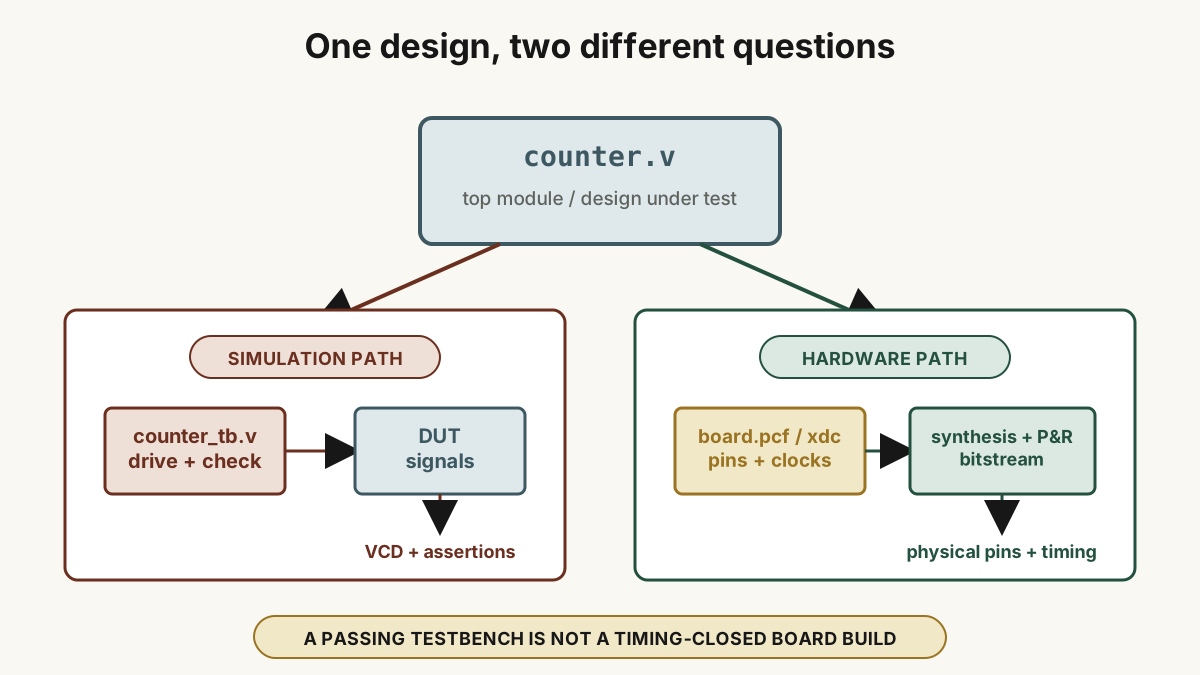
A Verilog file can contain one module, several modules, or simulation code. Tools read its declarations and build from the hierarchy root you select; naming the file top.v never selects the top by itself.
This compact project layout makes each engineering role visible:
counter-project/
├── counter.v          synthesizable design module
├── counter_tb.v       simulation top, stimulus, checks, VCD
├── board.pcf          board-revision pin bindings
├── timing.sdc         clock and timing intent, when the flow uses it
└── Makefile           repeatable simulation and build commands
The supplied lab includes counter.v, counter_tb.v, and a Makefile. Add the board.pcf only after selecting the exact board revision, because pin numbers, oscillator pins, reset polarity, LED polarity, package, and board naming can all change between revisions.
Verilog also permits a design module and testbench module in one file for quick work. Separate files make their different jobs obvious to both the engineer and the build system.
Select The Synthesis Top As The Hardware Root
The top module acts as the root of the hierarchy for one tool run. It owns the implemented design’s external ports and instantiates every child module below them. A software main() offers a rough navigation analogy, but hardware hierarchy gives the top its real meaning.
In the counter lab, counter can serve as the synthesis top because clk, reset, and count define the complete hardware interface. A board build can place a wrapper above it:
module board_top (
    input  wire       clock_100mhz,
    input  wire       reset_n,
    output wire [7:0] led
);
    wire [26:0] count;

    counter #(.WIDTH(27)) divider (
        .clk   (clock_100mhz),
        .reset (~reset_n),
        .count (count)
    );

    assign led = count[26:19];
endmodule
The wrapper converts board-facing names and active-low reset polarity into the counter’s reusable interface. It also selects slow counter bits that make LED changes visible. The selected board determines whether the LED assignment needs inversion.
Select the root in Yosys with hierarchy -top board_top or a synthesis command’s -top option. The official Yosys hierarchy documentation details that selection.
Let The Testbench Own The Simulated World
The supplied Icarus run selects counter_tb as its top. This portless module creates the entire simulated world: it generates a clock, controls reset, instantiates counter, waits for meaningful events, checks expected outputs, and ends the run.
The testbench performs five essential jobs:
- Instantiate the design under test and connect every relevant port.
- Generate clocks, resets, transactions, and corner-case stimulus.
- Sample outputs at times that respect the simulator’s scheduling rules.
- Compare observed values with explicit expectations and stop loudly on a mismatch.
- Record the message, assertion, waveform, seed, or transaction log needed to reproduce the run.
SystemVerilog, C++ around a Verilator model, cocotb with Python, and other simulator interfaces can all host the harness. Its ability to drive, observe, and decide the result makes it a testbench.
“Verilog” joins verification and logic in its name. The language can describe both the synthesizable circuit and the simulation environment, while the selected root and constructs give each module its role.
Bind RTL Names To Physical Pins And Timing
FPGA constraints connect top-level port names to the package and board. In the open iCE40 flow, a PCF can bind clock_100mhz or led[0] to a package pin, creating the literal metal-pad connection between RTL and the board.
A complete implementation can also specify:
- clock definitions, periods, waveforms, and generated-clock relationships;
- I/O standards, drive strength, slew, input and output delays;
- timing exceptions such as false paths and multicycle paths;
- placement regions or fixed resource locations; and
- tool- and device-specific implementation directives.
Toolchains divide this information differently. A PCF chiefly binds physical pins. An SDC carries timing intent. AMD/Xilinx XDC combines Tcl-based physical and timing constraints. An iCE40 nextpnr command can also receive its target clock frequency through --freq. Each format contributes a specific part of the implementation contract.
Follow One Clock Name Through Three Worlds
Consider clk. The synthesizable module consumes it in an edge-sensitive process. The testbench toggles it through simulated time. The board constraints connect it to the oscillator pin and define its implementation frequency.
input wire clk captures state on the selected edge.clk with delays and samples the updated state.The simulation path establishes behavior under driven cases. The implementation path binds that behavior to physical resources and closes timing. Together they connect the source-level design to an operating FPGA.
Keep One Strong Language Reference Beside The Project
The USC EE457 Verilog discussion supplies the language reference for the course:
USC EE457 — Verilog Discussion (PDF)
Read that discussion alongside the executable lab files. For normative SystemVerilog scope and terminology, consult the IEEE 1800 standard page. Later chapters return to this reference as their common language foundation.
Trace The Complete Project From Source To Pin
Name the synthesis root and simulation root. Identify what generates the clock in each world. Find the file that connects an LED port to a package pad and the constraint that states the clock requirement. Then follow the counter from its reusable module through automated simulation and into a timed physical implementation.