Seven Milestones Turn Logic Into Working Hardware
- Manipulate Boolean logic. Build switching functions until gates, truth tables, multiplexers, and shared terms become concrete tools.
- Draw the circuit in Logisim. Wire, toggle, observe, and debug the design while every connection remains visible.
- Express hardware in HDL. Use Verilog and SystemVerilog for combinational logic, clocked state, hierarchy, and automated checks; read VHDL when a project calls for it.
- Run a counter and its testbench. Combine the design, stimulus, expected results, and waveform into one repeatable simulation.
- Drive physical FPGA I/O. Choose the exact board revision, bind ports to pins, set electrical and clock constraints, build a bitstream, and observe the result.
- Open the CMOS layer. Connect transistor logic, timing, power, metastability, memory, and clocking to the digital structures above them.
- Continue into ASIC implementation. Extend the same design discipline through synthesis, physical design, signoff, packaging, and tapeout.
The route supports constant movement between layers. A surprising Verilog result sends you back to the circuit; a timing failure sends you back to the RTL; an ASIC question can reshape an architecture first explored on an FPGA.
Make Boolean Structure Visible First
Begin with AND, OR, NOT, XOR, multiplexers, decoders, adders, and simple state. Write truth tables, simplify expressions, and find the intermediate terms that multiple outputs share. Then route feedback through an explicit storage element and trace exactly what changes at each clock edge.
Logisim-evolution keeps the circuit in view. Toggle an input, watch a wire change, inspect a subcircuit, and repair a missing connection immediately. That direct feedback builds switching intuition before language syntax enters the work.
Logisim models the structure; the target FPGA adds physical propagation, clocking, routing, and device constraints. Use the schematic to understand the circuit, then let synthesis and timing tools show how the selected fabric implements it.
The site’s bubbles-free bit-serial multiplier advances this method: after the pipeline fills, one result bit leaves on every clock. Its visible circuit turns a computation schedule into something you can trace wire by wire.
Use HDL To Specify The Circuit
Verilog and SystemVerilog give the route its practical language: modules and ports, vectors and indexing, continuous assignments, combinational procedures, edge-triggered procedures, parameters, hierarchy, and testbench constructs. These elements support substantial FPGA systems and carry directly into ASIC flows.
Many existing designs use VHDL, so the ability to read it expands the codebases you can enter. Python strengthens the surrounding workflow by generating data, running tests, inspecting outputs, and driving verification frameworks. The RTL still defines the hardware.
Keep a language reference beside an active design. The project-anatomy chapter provides this course’s Verilog quick reference; use it to answer syntax questions that arise from the counter and its testbench.
Turn The First Design Into A Repeatable Result
Create a counter circuit and a testbench, compile both with Icarus Verilog, and run the simulation with vvp. Named design and test files, explicit reset and clock stimulus, automated checks, a VCD dump, and an expected terminal result turn one command into a complete workbench.
The counter defines the hardware. The testbench supplies its clock and reset, drives its inputs, and checks its outputs. Together they convert intended behavior into a result that another engineer can run, inspect, and extend.
Carry The Design Across Physical Pins
Simulation establishes the modeled behavior. FPGA implementation adds the device, board revision, clock source, top-level ports, package pins, I/O standards, timing requirements, power, connectors, and bitstream loader.
Choose the exact board revision before downloading constraints or running a loader; boards within one product family can assign clocks and LEDs to different pins. Make the first hardware result unmistakable: drive an LED from a slow counter bit or route a measurable loopback signal.
Write the hardware acceptance condition before the build: name the LED or pin, its approximate visible rate, the reset response, and the observations that separate an RTL problem from pin mapping or board detection.
Fast Feedback Opens The Deeper Engineering Path
The course map captures the transition in one memorable line:
Above: fun & cheap & easy.
Below: useful & career-focused.
Boolean play, a compact simulator, and one visible board result create fast feedback. That speed builds the intuition needed for harder work without first requiring a tapeout budget or a complete semiconductor curriculum.
CMOS study opens transistor behavior, noise margins, delay, dynamic and leakage power, clocking, storage, and physical implementation. ASIC tapeout adds technology libraries, design-for-test, floorplanning, power distribution, clock trees, extraction, timing and physical signoff, packaging, fabrication, and bring-up. Each domain can support an entire engineering career.
FPGA experience forms a powerful bridge. It joins clocked state, finite resources, synthesis, timing reports, constraints, I/O, and verification with short edit-build-test cycles. The ASIC path then adds its physics, manufacturing, and process disciplines.
Use Five Analogies To Reach The Hardware Model
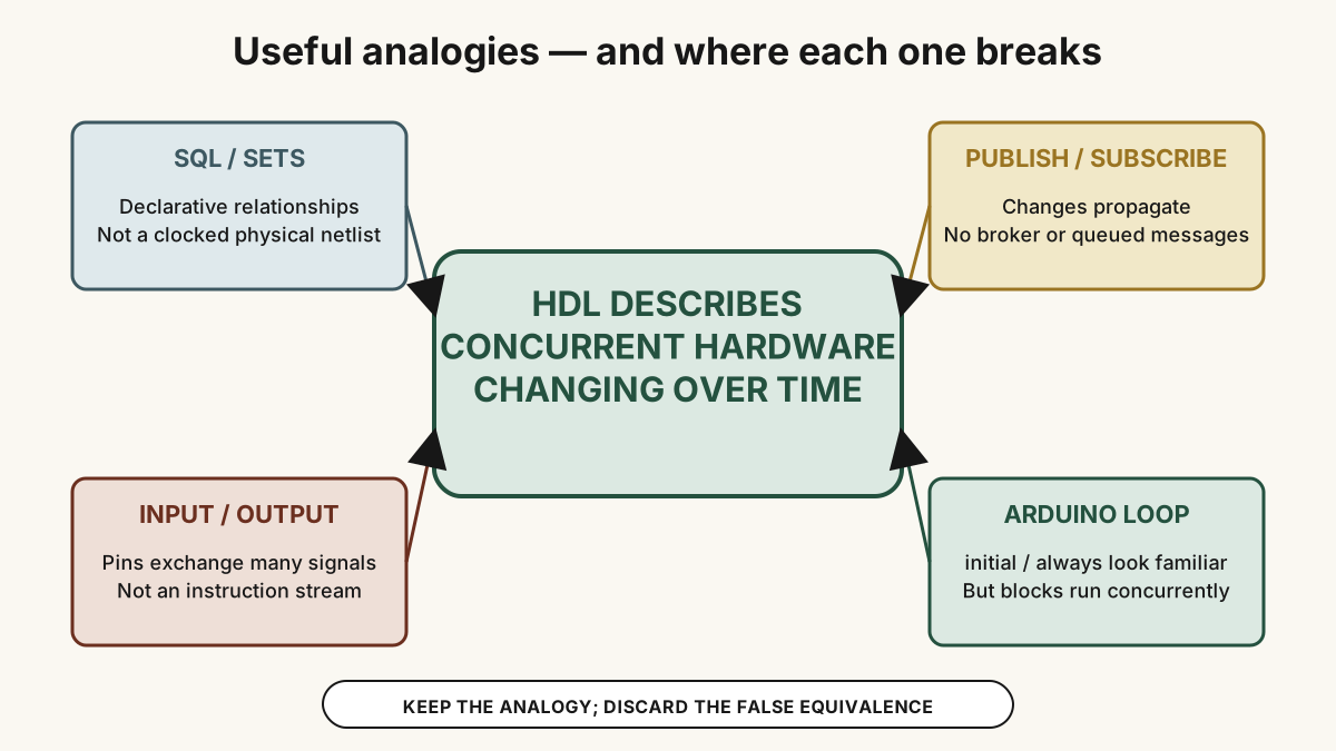
Familiar software models offer quick entry points into HDL. Use each analogy to establish one useful connection, then return to the circuit’s concurrency, timing, and finite resources.
Is it like Logisim?
The connection: both describe networks of logic, storage, and connections. A Verilog module can match a Logisim subcircuit, while a testbench automates cases once toggled by hand.
The hardware model adds: widths, signedness, clock and event semantics, hierarchy, parameterization, and simulation-only behavior. Synthesis transforms the written structure as it maps the design onto the FPGA.
Is it like SQL and set-based thinking?
The connection: SQL breaks the habit of spelling every operation as an imperative loop. An HDL expression likewise describes a relationship that hardware maintains whenever its inputs change.
The hardware model adds: RTL allocates finite state, operators, and connections with clock and timing consequences. Two equivalent equations can map to different hardware cost or latency.
Is it like publish/subscribe?
The connection: a signal change can awaken multiple dependent processes, and one produced value can fan out to several consumers. Event-driven simulators make that concurrency visible.
The hardware model adds: fanout consumes electrical and routing resources, and clock-domain crossings require explicit treatment. Nets carry signals directly rather than queued messages with implicit buffering or backpressure.
Is it like high-throughput I/O?
The connection: FPGA pipelines accept and transform streams continuously, while many pins or serial lanes operate concurrently. The fabric need not fetch every elementary operation through one CPU instruction stream.
The hardware model adds: device, I/O standard, board, clocking, protocol, timing closure, and architecture determine the rate. Width, frequency, serialization, latency, and backpressure together define throughput.
Is it like Arduino setup() and loop()?
The connection: in simulation, an initial block begins once, while an always block reacts repeatedly according to its timing or event control. Arduino programmers can use that distinction as an entry point.
The hardware model adds: every initial and always block runs as its own concurrently scheduled process, while statements inside one block keep their order. Synthesizable meaning depends on the construct and tool. Use always_comb for combinational intent and always_ff @(posedge clk) for clocked intent when SystemVerilog support allows, and learn blocking and nonblocking assignment rules directly.
Predict, Run, And Read The Result At Every Layer
Before each tool run, write an informed prediction: the truth table will match; the counter will wrap after sixteen states; the waveform edge will follow reset; the LED will toggle from a divided clock; this timing path will limit the design. Then run the tool and compare the result directly with that prediction.
This loop connects a Logisim switch to a physical FPGA and gives every tool result an engineering meaning. It also prepares the later counter recreation, where datasheet behavior becomes a complete set of executable checks.