The Fab Builds the Physical Possibilities
A fabrication plant forms devices and patterned interconnect on semiconductor wafers through deposition, lithography, etching, implantation, and related process steps. The finished geometry fixes where transistors and metal exist.
Integrated circuit names the broad category. An application-specific integrated circuit, or ASIC, targets a particular application or family. Microprocessors, GPUs, and FPGAs also belong to the integrated-circuit family. The FPGA distinguishes itself through an architecture that invites later configuration.
Industry history credits Xilinx cofounder Ross Freeman with the FPGA concept, and Xilinx launched the XC2064 in 1985 as the first commercial FPGA. “Field-programmable” gives the user control over the configured function after manufacture—at a lab bench, inside a product, or during deployment.
The ASIC Flow Commits Geometry
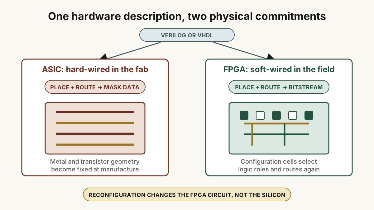
ASICs become hard-wired in the fab. Verilog or VHDL can start a digital ASIC flow. Synthesis creates a technology-mapped netlist. Physical design establishes the floorplan and power network, places cells, builds clock trees, routes signals, and closes timing and physical-verification requirements. GDSII or OASIS signoff data describes geometry for masks in the selected manufacturing process.
Three distinct ingredients drive that flow:
Foundry, node, program, and agreement determine process access. The public SkyWater SKY130 PDK documentation supplies a concrete 130 nm reference. A PDK provides process information; a standard-cell library provides characterized logic cells; a shuttle program organizes shared manufacturing access.
The FPGA Flow Selects Existing Resources
FPGAs become soft-wired in the field. Synthesis maps Verilog or VHDL onto primitives in one FPGA family. Place-and-route chooses physical sites and interconnect. The resulting bitstream records those choices.
Configuration memory controls LUT contents, routing switches, I/O modes, clock resources, embedded memories, arithmetic blocks, and other features that already occupy the silicon. A new bitstream reconnects those resources without manufacturing another chip.
That reloadability gives an FPGA extraordinary experimental range. Many devices accept new configurations in milliseconds to seconds, depending on image size and interface. One FPGA can even configure another. The Ethernet-to-adjacent-iCE40 project receives network data, stores it, and drives a neighboring FPGA's configuration pins.
A Spatial Graph Computes Many Functions at Once
A processor often presents computation as an instruction stream. An FPGA presents a spatial network of Boolean functions, storage elements, memories, arithmetic blocks, and wires that operate concurrently.
A forest of Boolean trees captures the structure. Shared branches prevent exponential duplication: designs reuse intermediate results, register boundaries, buses, memory, hierarchy, and specialized blocks. Synthesis maps that shared graph onto resources that the selected device supplies.
Combinational logic produces bits and vectors from current inputs and state. Flip-flops let those values persist and drive the following cycle.
The D Flip-Flop Separates Current State From Next State
A positive-edge-triggered D flip-flop samples D at the active clock edge and holds that value on Q until the next active edge or control event. Device designers may realize that behavior with latches, transmission gates, multiplexers, or other transistor structures.
Synchronous design follows one clean sequence:
- Register outputs and external inputs enter the combinational network.
- The network calculates candidate next values.
- Receiving flip-flops capture those candidates at the active clock edge.
- The captured values drive the following cycle as current state.
Current state remains visible before the edge. Combinational equations calculate candidate next state from it. The edge commits that candidate. A nonblocking assignment in clocked Verilog expresses the same old-value/new-value sequence.
Massively Parallel Reactive Programming Opens the Door
Massively parallel reactive programming gives software developers a useful first handle. Physically distinct resources respond to inputs and state during the same clock interval, while a processor time-multiplexes a smaller set of execution units across many operations.
Modern CPUs also contain cores, pipelines, SIMD units, caches, accelerators, and asynchronous I/O. FPGA strength emerges when a computation rewards deterministic spatial pipelines, unusual word widths, many simultaneous I/O lanes, cycle-level timing, or a datapath outside a processor's instruction machinery.
Verilog modules and processes exist concurrently. Continuous assignments react to their dependencies. Statements inside each procedural block follow the language's execution semantics. Chapter 2 now places that model inside the LUT, flip-flop, and routing fabric.
Carry Two Distinctions Forward
ASIC: physical design commits device and interconnect geometry for fabrication.
FPGA: the factory supplies the physical fabric, and the bitstream selects functions and routes inside it.