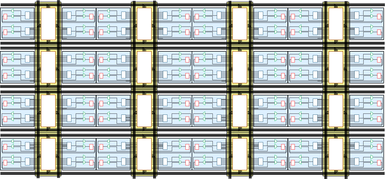
Repetition Creates Placement Freedom
A conventional FPGA repeats programmable logic across a large array. Repetition helps manufacture the chip and gives implementation tools many candidate sites. A compact Boolean function can occupy one local site; a larger datapath can spread across neighboring regions.
I/O banks, block memories, arithmetic or DSP units, clock networks, configuration logic, and sometimes high-speed transceivers or processor cores interrupt that regular array. Their fixed positions make the fabric intentionally nonuniform.
Five resource classes define the top-level machine:
- programmable logic computes compact Boolean functions and holds local state;
- configurable interconnect carries signals among resources;
- I/O connects top-level ports to package pins and electrical standards;
- memory, arithmetic, clocking, and other hard blocks perform structures that LUT fabric would implement less densely or slowly; and
- configuration state assigns every resource its role.
Intel's FPGA architecture overview shows one first-party realization of those categories. Other families arrange them differently.
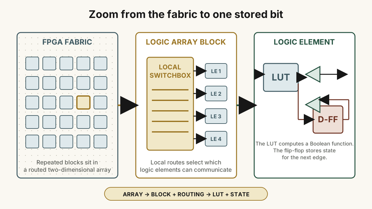
Vendor Dialects Name the Same Structural Need
A repeated region needs programmable Boolean logic, registers, carry or control resources, and local routing. Intel calls groupings LABs and may place LEs or ALMs inside them. AMD uses CLB, slice, LUT, and flip-flop. Lattice families commonly expose logic cells or slices around LUT/register pairs. Each generation chooses its own grouping.
Vocabulary never supplies a universal size. One LAB does not imply one byte of Boolean trees, and eight bits do not define an architectural unit across FPGA families. The target architecture manual gives the resource counts, carry chains, shared controls, and packing rules.
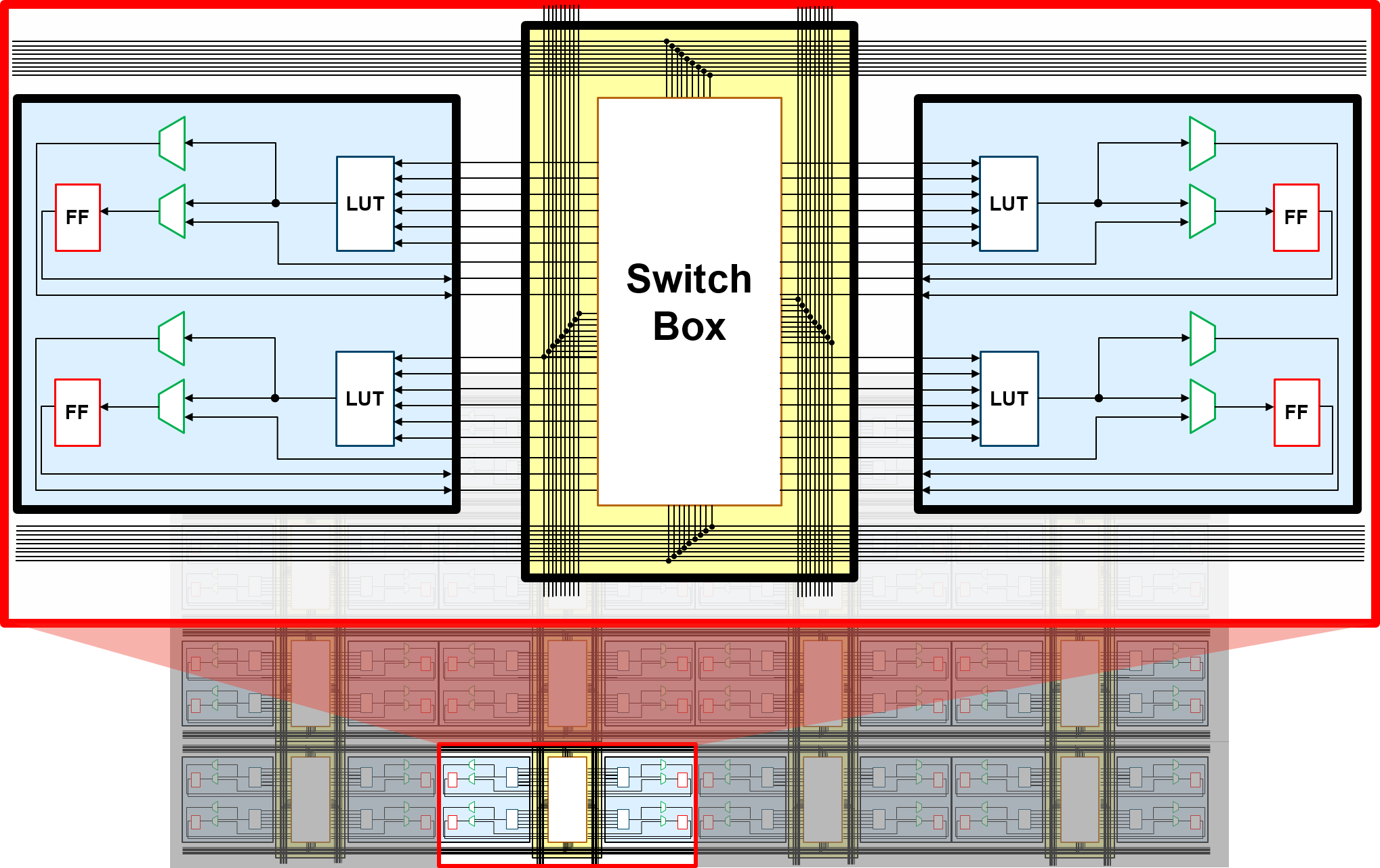
The Switchbox Completes the Logic
Configurable switches deliver inputs and carry outputs among local wires, neighboring blocks, longer row or column tracks, I/O, memories, and other resources. Without those routes, a LUT has no useful circuit around it.
Short connections serve nearby producer-consumer paths. Longer wires cross regions. Dedicated networks carry clocks, resets, enables, and carry signals under specialized rules. Place-and-route searches this finite graph for legal sites and paths.
Two logically equivalent RTL descriptions can therefore consume different resources or reach different timing. Placement, route length, switch count, and special-resource use turn Boolean equations into a physical circuit.
A LUT Turns Configuration Bits Into a Function
A k-input lookup table stores one result for each of its 2^k input combinations. Live input bits select one configured result, so the LUT implements a compact Boolean function.
Synthesis simplifies logic, shares or duplicates terms, recognizes arithmetic and multiplexing structures, and maps the transformed graph into available LUT shapes. Larger functions span several LUTs and routes.
Specialized resources extend the LUT. Carry chains accelerate arithmetic. Block RAM stores data densely. DSP blocks multiply and accumulate with less general fabric. Clear RTL lets synthesis choose these resources while tool reports expose the choice.
The Flip-Flop Carries the Function Through Time
Many logic elements place a flip-flop beside the LUT. The LUT calculates a combinational value; the flip-flop captures a selected value at the clock edge and holds it. Local multiplexers can choose combinational output, registered output, carry output, or another family-specific path.
This pairing implements the “D is next; Q is current” model and makes pipelining practical. One region computes a stage, nearby registers hold it, and the next region continues during the following cycle.
Repeating LUT/register pairs lets an FPGA host many pipelines and state machines at once. The bitstream activates and joins resources; clocks and inputs drive the resulting circuit.
Read the Fabric at Three Scales
Each scale answers a distinct implementation question:
- Chip scale: locate logic, memory, DSP, I/O, clocking, and hard subsystems.
- Block scale: inspect one repeated logic group and its shared controls or carry resources.
- Element scale: trace connections among a LUT, register, local multiplexers, and dedicated paths.
A block diagram frames the question; the family architecture manual and implementation reports supply exact device detail.
RapidWright's FPGA Architecture Basics gives a concrete view of AMD/Xilinx Series 7 resources and terminology.