The Complete Path
Fourteen source files cross the physical network edge, packet framing, on-chip storage, two FPGA families, and the target-device configuration sequence. The packet does not stop at a processor or software API; it becomes new hardware behavior in the neighboring device.
ARP Without A CPU In The Datapath
The FPGA receives RMII dibits, finds the start-of-frame delimiter, collects bytes, recognizes the relevant ARP request and destination, captures the requester addresses, and constructs its response entirely in RTL.
The transmit path emits the preamble, destination and source MAC addresses, ARP fields, padding, and frame CRC. It locks the parser while it sends the response, giving the design one explicit transaction at a time.
Inspect the ARP recognition and trigger and the response construction.
A Fixed Packet Layout Becomes FPGA Memory
The receive path checks the Ethernet IPv4 EtherType and destination IP address, then takes byte 42 as the start of its fixed-layout payload. Packet position determines each RAM address as incoming dibits arrive.
This purpose-built transport eliminates a general network processor from the datapath. For its selected sender, address, and image layout, Ethernet fields lead directly to the memory that will configure the target FPGA.
Inspect the EtherType, destination-IP, fixed-offset, and RAM-write path.
The Neighboring FPGA Is The Payload Destination
After RAM receives the image, the controller drives the Lattice slave-configuration interface directly: CRESET_B, SPI_SCK, SPI_SI, and SPI_SS_B, while CDONE returns target status.
The design selects the iCE40LP384 image length, switches the same RAM from network writes to configuration reads, sequences reset and data, and clocks the stored image into the adjacent device.
Inspect the configuration-pin wiring, RAM selection and LP384 length, and the final configuration outputs.
The Linux Side Is A Real Control Shell
The host program loads a 7,337-byte processed image and sends it over UDP to the device address and port. Its epoll loop unifies the socket, terminal, signal handling, and XCB events.
The same program creates an XCB window and EGL/OpenGL ES 2 context. Its active render path sets the viewport and clears the 64-pixel window red, joining network control, native events, and a GPU-backed operator surface in one process.
Inspect image loading, UDP transmission, EGL setup, and the active draw routine.
Source Map
Fourteen files and eight recorded revisions preserve the full development path. A later related Gist continues it as Working reprogrammer.
To build the foundations for this multi-file system, begin with Verilog modules, top modules, testbenches, and constraints, then follow the Yosys, nextpnr, and IceStorm path from RTL to a board bitstream.
The Packet Ends As New Hardware
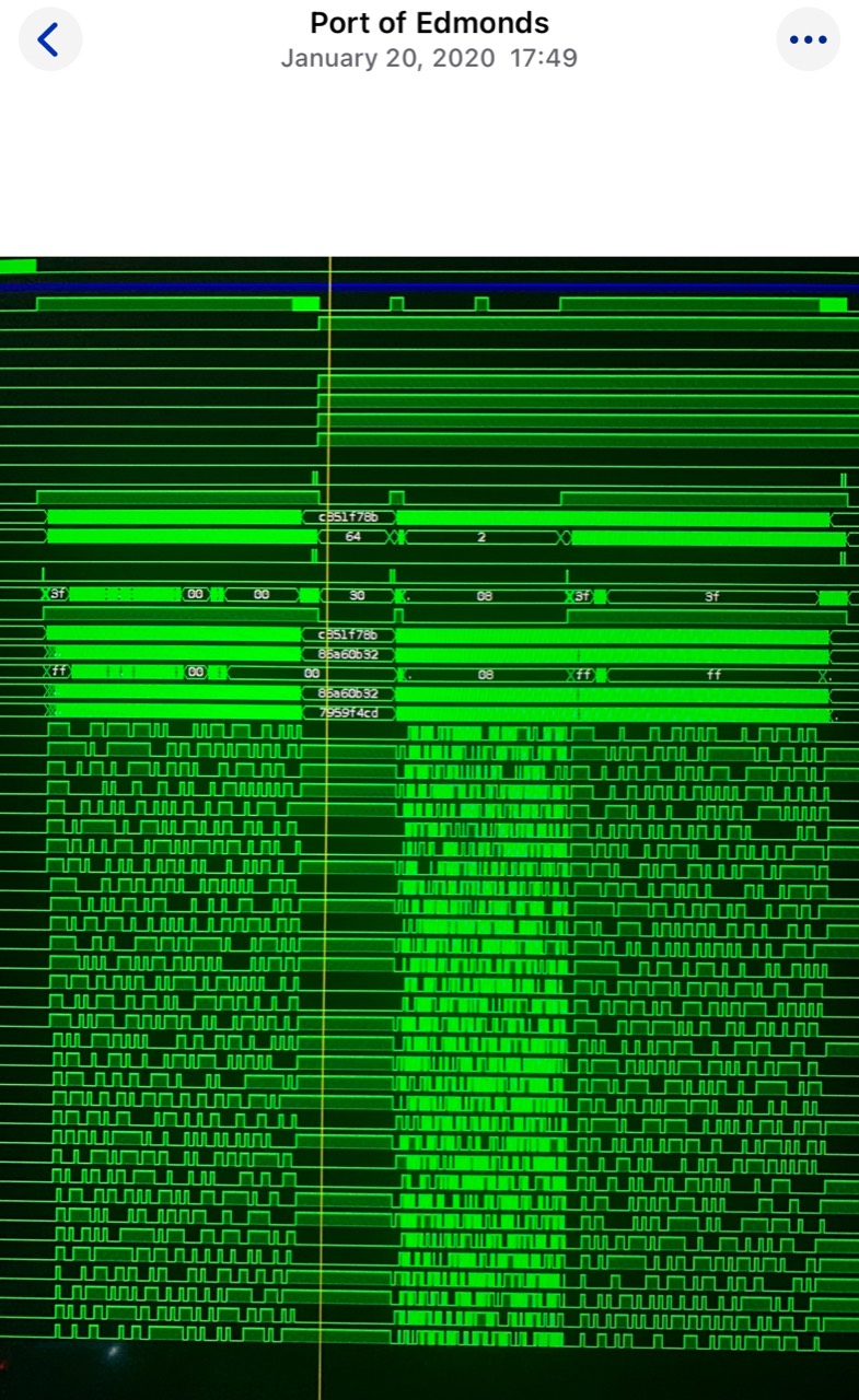
The 2020 system joins PHY and RMII handling, direct ARP behavior, fixed-layout network ingestion, on-chip image storage, configuration-pin sequencing for an adjacent Lattice FPGA, a Yosys/arachne-pnr/IceStorm build path, and a Linux control utility.
That architecture remains a powerful route to field-programmable products: place network handling and image storage in one device, then make neighboring low-cost FPGAs replaceable over the same physical system. The source invites a modern board port, a richer transport protocol, or a product-specific configuration controller.