Keep Every Wire, Bit, And State Transition Visible
Logisim keeps the circuit in view. A wire carries a value, a component transforms it, and a clocked component retains state. Single-step control reveals exactly which bit moved.
The public bubbles-free serial multiplier uses legacy Logisim 2.7.1 so its streaming schedule and repeated serial-adder structure remain directly inspectable. The actively maintained Logisim-evolution project provides a current cross-platform environment for designing and simulating digital logic. Both routes keep the circuit concrete.
Turn One Multiplexer Into One Address Bit
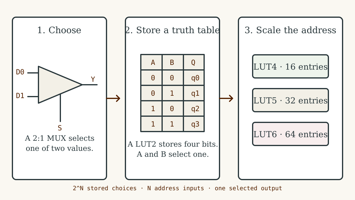
A 2:1 multiplexer accepts two data inputs and one select input. The select bit chooses which data input reaches the output:
Y = S ? D1 : D0
Store two configuration bits at D0 and D1, then use the select input as an address. LUT1 lets one input choose one of two stored truth-table values.
The stored pair 1, 0 implements an inverter, while 0, 1 implements a buffer. 0, 0 and 1, 1 implement constant zero and constant one. Those four configurations cover every Boolean function of one input.
Hands-on companion: the physical MUX-tile alphabet turns selector inputs, constants, routes, intersections, orientation, and composition into fabricated PCB parts that learners can manipulate before moving into stored LUT bits.
The published photographs document real pieces and palm-scale assembly. Powered operation and classroom study define the next physical program.
Grow The Same Selector Tree Through LUT6
A LUT with N inputs stores 2^N output bits. Its input vector addresses one stored choice.
Draw LUT2 as a two-level multiplexer tree: one select bit chooses within each pair, and the second chooses between the pair results. LUT3 adds another level. Each FPGA family can pack or share its physical resources differently while preserving the truth-table definition.
The 2020 article MUX Algebra expresses this LUT2 tree as nested conditional notation, enumerates all 16 two-input Boolean functions, and defines a compact four-bit source-pointer encoding.
Meet LUT4 As A Named iCE40 Primitive
Lattice’s iCE40 technology library exposes SB_LUT4. Four inputs address a 16-bit LUT_INIT value, and the selected bit drives the output. The official iCE40 Technology Library documents both the primitive and the input-to-LUT_INIT mapping.
The teaching diagram therefore connects directly to a named device primitive with a configuration word and an exact address convention.
Use LUT5 And LUT6 Inside AMD/Xilinx Slices
AMD’s 7 Series and UltraScale configurable-logic documentation describes a 6-input LUT that operates as one LUT6 output or as two LUT5 outputs with shared inputs. The 7 Series CLB overview (UG474) and UltraScale CLB overview (UG574) place those modes inside complete slices.
FPGA families from iCE40 onward combine truth tables with distinct packing, carry chains, storage, distributed RAM, routing, and slice organization. Across those differences, a compact stored truth table plus physical routing remains a recurring unit of reconfigurable hardware.
Let The LUT Open The Larger Architecture
A lookup table explains configurable local Boolean choice. Cartilage extends that primitive into a spatial region that owns its boundary, receives a replacement image through a local reconfiguration port, composes a daughter region, and carries configuration transport inside the same fabric.
The learning path now moves through physical gain, output drive, clock and event distribution, state machines, timing closure, metal wires, nested components, and runtime creation of an adjacent daughter region. The LUT supplies the first tile of that complete architecture.
Build The Selector Tree Yourself
- Place one 2:1 multiplexer in Logisim and drive both select states.
- Tie its data inputs to two constants, then configure inverter, buffer, zero, and one.
- Assemble LUT2 from three multiplexers and four stored bits.
- Program AND, OR, XOR, and a 2:1 MUX as four-bit LUT2 truth tables.
- Check your address order against the official
SB_LUT4LUT_INITtable before assigning bit numbers.
Carry the visible logic into Verilog, simulation, synthesis, and a programmed board, then use Cartilage to make physical distribution and regional ownership explicit.