Turn Complementary Devices Into A Restoring Stage
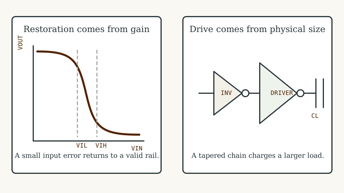
A complementary CMOS inverter pairs a pull-up device with a pull-down device. A low input activates the high output, a high input activates the low output, and the transfer curve moves sharply between those stable regions.
The MIT inverter-basics lecture develops the voltage-transfer characteristic, noise margins, and sizing that govern digital inverter behavior. UC Berkeley’s CMOS transistors and logic lecture marks the input thresholds where the voltage-slope magnitude reaches one.
Use Transition-Region Gain To Rebuild 0 And 1
The transfer curve becomes steep through its transition region. There, a modest input change produces a larger output change with opposite polarity, and the local slope magnitude exceeds one across part of a valid digital transfer curve.
This gain restores logic levels: a degraded low input produces a strong high output, and a degraded high input produces a strong low output. A two-inverter buffer restores the original polarity while sharpening both levels. MIT’s Computation Structures notes connect that greater-than-one gain region to noise margins and a valid combinational-device transfer characteristic.
Restoring gain makes “0” and “1” compositional across long signal chains by removing accumulated noise and voltage loss at each stage.
Pay The Resistance-Capacitance Cost Of Every Transition
The next stage’s input gates, the wire between stages, and the output structures all contribute capacitance. Every voltage transition moves charge, and finite source resistance sets how quickly the driver can deliver or remove it.
A first-order delay model captures the central trade:
delay ∝ Rdriver × Cload
Device choice, input slew, output load, process, voltage, temperature, interconnect, and characterization model refine the exact delay. Every schematic arrow therefore carries an electrical cost, and engineers size its driver for the expected load.
Scale A Buffer Chain To Reach The Load
Two inverters in series preserve polarity and form a buffer. When a compact logic stage must drive a much larger capacitance, a chain of progressively larger inverters distributes that effort across several stages.
Larger devices occupy area, add capacitance, and consume dynamic switching energy. A driver chain turns area and energy into a controlled transition-time and delay budget at a specific fanout.
Give Every Boundary A Driver And A Known Load
“Output driver” can name a stronger internal buffer, an FPGA I/O cell, a pad driver, a board-level line driver, or another physical interface. Here it means the stage that presents a valid transition to a known load.
Cartilage cell roles define logic, while clocks, events, resets, configuration edges, and application signals require implemented paths with bounded fanout, slew, delay, and restoration. The browser and RTL establish the logical mechanisms; transistor sizing and physical driver closure supply the next implementation layer.
Distribute One Restored Edge Across The Fabric
Once one driver moves one bounded load, the architecture must carry an event to hundreds or thousands of destinations while controlling the arrival difference between the nearest and farthest loads.
The next chapter expands one transfer curve into clock, event, and reset networks—buffer trees, H-trees, grids, clock roots, leaves, and regional distribution.