00
Positive I: the unrotated complex lane.
One-pin Weaver radio · exact signal path
Four quadrature mixers collapse onto one programmable FPGA RF output. Physical27 carried that phase-domain sum through N16 and a resonant tank, returning 8,592 checked QPSK bits with no observed errors.
Two baseband streams—SDM(I) and SDM(−Q)—pass through the first +7.5 MHz quadrature Weaver conversion. Their two one-bit results drive a four-state selector that realizes the two 216 MHz carrier mixers and adds them directly in phase. The summator emits one RF phase instead of separate analog I and Q voltages. N16 switches that phase high or high impedance, and the resonant network turns those timed charge impulses into the narrowband waveform.
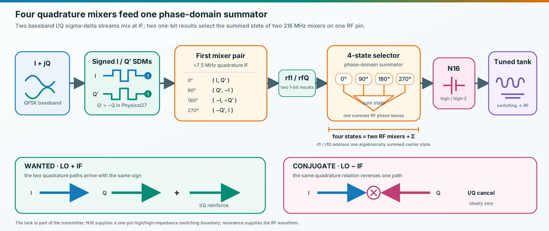
A Weaver transmitter contains two quadrature mixer pairs: the first converts baseband I/Q to an intermediate frequency, and the second converts those two results to RF. Together they produce four mixer products. I built their signs as coordinated one-bit rotations instead of four standalone multiplier blocks.
Let Q′ denote the selected Q polarity; Physical27 uses Q′ = −Q. For each +7.5 MHz quadrant, the first mixer pair produces (I,Q′), (Q′,−I), (−I,−Q′), or (−Q′,I). These two one-bit intermediate signals control the four-state selector. Each selector state performs the phase-domain sum of the second two mixer products at 216 MHz.
Using the sign convention that reinforces the upper branch, the continuous-time equivalent is I1 = I·cos(IF) − Q′·sin(IF), Q1 = I·sin(IF) + Q′·cos(IF), and s = I1·cos(LO) − Q1·sin(LO). Expanding the products leaves I·cos(LO+IF) − Q′·sin(LO+IF); the LO−IF cross-products cancel.
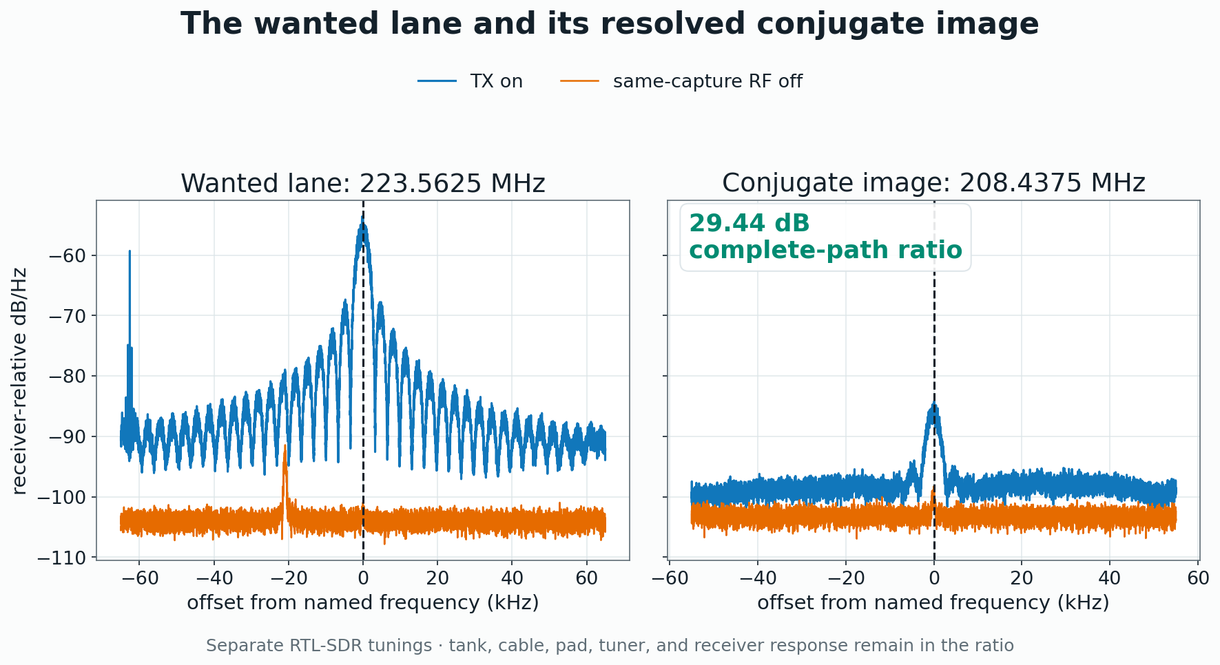
For Physical27, the 216 MHz carrier, +7.5 MHz whole-word rotation, and +62.5 kHz lane rotation place the wanted signal at 223.5625 MHz. The corresponding true RF conjugate image lies at 208.4375 MHz. The complete physical path measured the wanted lane 29.44 dB above that image.
An on-FPGA PRBS16 generator creates the payload. Its 16-bit register starts at 0x1D2B. At each symbol advance, the register computes its new low bit as p15 ^ p13 ^ p12 ^ p10:
shared_prbs_q <= {shared_prbs_q[14:0],
    shared_prbs_q[15] ^ shared_prbs_q[13]
    ^ shared_prbs_q[12] ^ shared_prbs_q[10]};
Lane 62 specializes the generated tap formula to {p5 ^ 1, p7} and maps those two bits to four cardinal states: 0=+I, 1=+Q, 2=−I, and 3=−Q. A symbol therefore adds 0, 8, 16, or 24 to the lane’s five-bit phase, which produces exactly a 0°, 90°, 180°, or 270° turn around its 32-point complex waveform.
00Positive I: the unrotated complex lane.
01Positive Q: one quarter-turn forward.
10Negative I: one half-turn.
11Negative Q: three quarter-turns.
The lane machinery runs at 108 MHz and streams each signed word least-significant bit first across 16 clocks, so its complex sample rate is 6.75 MS/s. In the 25 kHz plan, lane 62 contributes a +62.5 kHz rotation. The QPSK state advances once per 2,048 words, giving 108 MHz / 16 / 2048 = 3,295.8984375 symbols/s.
The five-bit phase selects one of 32 signed I/Q points whose magnitude and initial phase come from compile-time tank-preemphasis constants. Physical27 enables the 17-sample serial moving sum, reconstructs its signed result, divides by 16 with an arithmetic shift, and applies the single-lane gain shift of seven. No host waveform file and no runtime wide multiplier sit in this path.
The PRBS register advances on a symbol tick, while the lane registers consume that advanced state on the following word boundary. A pending flag crosses that boundary, and the payload epoch increments only when the lane applies the new symbol. That small timing distinction lets the telemetry name the symbol driving the physical lane rather than a nearby PRBS state.
Read the active lane, PRBS, moving-sum, SDM, and Gray-rotation RTL. The PRBS transition is at lines 394–425, the applied lane symbol at 481–524, and the 32-point waveform selection at 545–598.
The lane finishes as ordinary signed 16-bit I and Q samples. Each component then enters its own first-order sigma-delta modulator. The modulator decides from the sign of its accumulated error, emits that decision, and subtracts the matching positive or negative full-scale feedback from error + sample:
wire quantizer_d = !error_q[17];
wire signed [18:0] feedback_d = quantizer_d
    ? 19'sd32768 : -19'sd32768;
wire signed [18:0] corrected_d =
    $signed({error_q[17], error_q})
    + $signed({{3{sample_i[15]}}, sample_i})
    - feedback_d;
The same quantizer_d becomes both the emitted bit and the feedback choice for that clock. The emitted decision and the error accumulator agree on every cycle. Over time, the density and pattern of ones carry the signed sample while the switching sequence moves quantization error away from the signal.
Physical27 inverts Q before the second modulator. After that point the datapath contains only i_sdm_bit and q_sdm_bit, plus their internal error states for telemetry. Together, those two bits form a complex phase word that the rotation and RF-clock mapping consume directly.
A 216 MHz phase accumulator advances by 5 modulo 144. Its frequency is therefore 216 MHz × 5 / 144 = 7.5 MHz. Thresholds at 36, 72, and 108 divide that accumulator into four equal quadrants.
Each quadrant permutes or inverts both SDM bits together:
| DDS quadrant | Selector word | Complex operation |
|---|---|---|
| 0 | (I, Q) | No additional turn |
| 1 | (Q, ~I) | Quarter-turn |
| 2 | (~I, ~Q) | Half-turn |
| 3 | (~Q, I) | Three-quarter-turn |
This whole-word rotation implements the first quadrature mixer pair. The datapath transforms I and Q together instead of processing them in separate time slots. One DDS quadrant transforms the complete two-bit state on every 216 MHz edge. Physical27 leaves the later optional 90° summator rotation disabled.
The arithmetic also makes the target frequency easy to follow: lane 62 contributes +62.5 kHz, the common DDS contributes +7.5 MHz, and the four-phase PLL supplies the nominal 216 MHz carrier. Their sum is the 223.5625 MHz wanted lane.
The iCE40 PLL produces nominal 216 MHz outputs separated by 90°. Their inversions supply the other two phases. The four-state selector maps the two intermediate bits directly onto those clocks:
wire p1 =  pll_216mhz_i;
wire p2 =  pll_216mhz_90_i;
wire p3 = ~pll_216mhz_i;
wire p4 = ~pll_216mhz_90_i;
assign modulated_rf_o = selector_i_i
    ? (selector_q_i ? p1 : p4)
    : (selector_q_i ? p2 : p3);
11 selects 0°, 01 selects 90°, 00 selects 180°, and 10 selects 270°. Each state equals the algebraic sum of the two 216 MHz carrier-mixer products for that input pair. The selector is therefore the phase-domain summator, and its one output is already the combined RF signal.
The top level derives both PLL phases from the 12 MHz board reference and also divides the in-phase output to make the 108 MHz lane clock. The Physical27 timing declarations used 216.03 MHz for the fast domain; the completed HX8K route reached 244.20 MHz on that constraint.
Read the four-state selector that performs the phase-domain sum at lines 423–437, and read the PLL and telemetry top at lines 140–176.
Physical27 uses the pMOS side of an iCE40 SB_IO. Its data input stays at one, and the phase-selected RF bit controls output enable:
SB_IO #(
    .PIN_TYPE(6'b101000), .IO_STANDARD("SB_LVCMOS"), .PULLUP(1'b0)
) rf_output_io (
    .PACKAGE_PIN(rf_out_o), .D_OUT_0(1'b1),
    .OUTPUT_ENABLE(physical_enable)
);
When output enable is one, N16 drives high. When it is zero, N16 becomes high impedance; it does not pull the tank low. PLL lock, reset, datapath readiness, the one-shot gate, and the selected carrier state all stand between the FPGA image and that enable signal.
The one-shot counter permits 324,000,000 cycles at 108 MHz, nominally three seconds. A configuration-initialized started latch prevents reset or PLL loss from starting a second burst. Outside that bounded interval, the RF pad remains high impedance. Physical27 also left the optional final output-enable complement disabled.
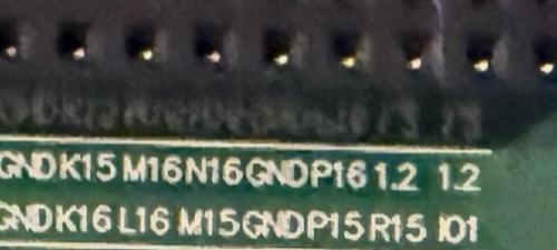
RF_OUT to this package pin.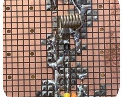
The one-pin architecture concentrates the programmable RF path on one FPGA output. Power, ground, the 12 MHz reference, configuration wiring, telemetry, the resonant network, coupling, and the receiver complete the radio.
Read the one-shot and N16 boundary RTL. The counter is at lines 4–50 and the SB_IO boundary at lines 256–264.
A high/high-impedance square switching sequence contains sharp edges and many frequency components. The tank accepts those impulses, stores energy in its electric and magnetic fields, and favors a narrow region around its resonance. The physical output is therefore a collaboration between RTL timing and resonant matter.
Five NanoVNA sweeps placed the median S21 maximum at 220.783 MHz and the upper half-power crossing at 223.719 MHz. The 223.5625 MHz QPSK lane sits about 156 kHz inside that upper crossing, where interpolation placed median S21 at about −23.22 dB at the existing calibration plane.
A separate five-repeat 50–300 MHz sweep covered both Weaver products. Its coarse complex interpolation made S21 about 7.95 dB higher at the 223.5625 MHz wanted lane than at the 208.4375 MHz image, so the tuned network clearly favored the wanted frequency. The NanoVNA and SDR used different instruments and reference planes, so the 29.44 dB complete-path ratio retains both physical transfer and digital Weaver contributions.
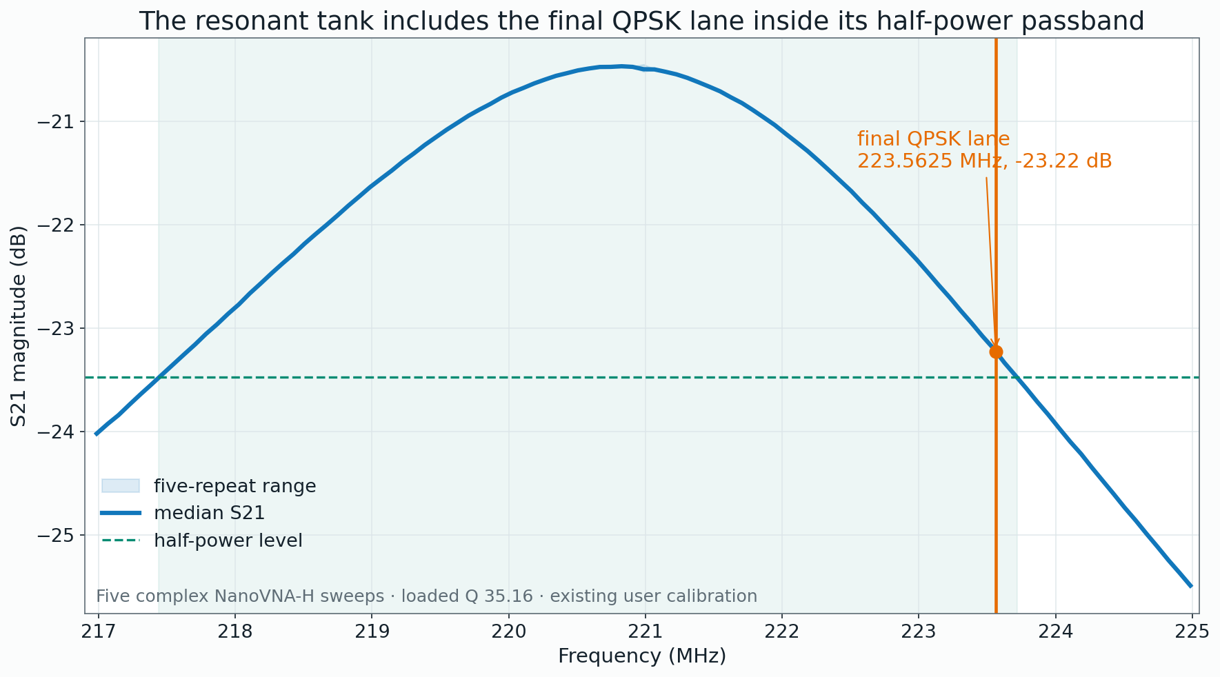
That local S21 measurement characterizes transfer at the existing calibration plane. Calibrated RF power at N16 or the tank output requires a power measurement at those planes. The earlier tank sketch notes about −15 dBm beside a 7.5 kΩ coupling value; the sketch names neither its load, reference plane, nor instrument settings. July used a different frequency and recorded coupling value. Removing or substantially changing the tank changes the transmitter.
The v10 telemetry frame includes the payload epoch and exact applied symbol, reconstructed pre-SDM I and Q, both SDM decisions and error states, the +7.5 MHz DDS phase, the two selector bits, burst state, and the real N16 enable. The payload fields come from the same update that drives the lane, so they do not infer the symbol from a later receiver decision.
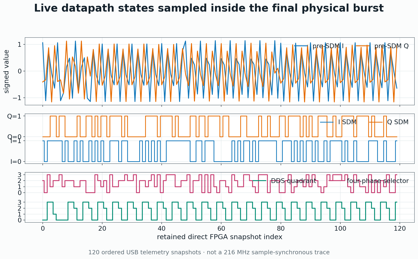
The horizontal axis follows USB snapshot order rather than nanoseconds or a sample-synchronous 216 MHz logic-analyzer trace. USB transport skips enormous numbers of FPGA clocks between records. The plot connects real internal states in causal order; RF-edge timing, PLL phase error, and setup and hold behavior at N16 require a different measurement.
V10 preserves the original transmitter's defining architecture: four quadrature mixers terminate in a phase-domain summator whose two one-bit controls select the final RF state on a pMOS-only FPGA pad. The rebuilt baseband and IF implementation carries a finite, internally generated digital message and names the state that drives the pin.
| Stage | April 2025 mod_apr20.sv | Physical27 v10 |
|---|---|---|
| Complex source | Opposing 32-bit sawtooths | PRBS16 QPSK on a signed 32-phase lane |
| One-bit conversion | Two threshold accumulators | Two signed first-order SDMs with one consistent decision and feedback value |
| First mixer pair | Adjacent phases of a Johnson counter used specifically as the quadrature IF oscillator | One +7.5 MHz quadrant rotates the complete two-bit word |
| Phase-domain summator | rfI/rfQ select the summed state of two 216 MHz mixers | The same four-state RF summation |
| Pad behavior | Constant high data with phase-controlled output enable | The same high/high-impedance pMOS boundary, now behind PLL/reset and one-shot gates |
| Internal observation | No applied-symbol epoch | Direct symbol, epoch, I/Q, SDM, DDS, selector, and physical-enable telemetry |
The April 2025 source and v10 share an architecture across distinct builds. Lines 653–725 show the baseband SDMs and IF mixer pair; lines 711–736 show the phase-domain summator; and lines 479–493 show the pMOS SB_IO. V10 replaces the baseband and IF implementation while keeping the four-mixer architecture, summator, and physical boundary.
Read the April 2025 mod_apr20.sv beside the active v10 channelizer and modulation RTL.
The Physical27 build uses Yosys 0.52, nextpnr-ice40 0.7-1+b2, IceStorm icepack, an iCE40HX8K in the CT256 package, and nextpnr seed 1. It reads the same six SystemVerilog files in the same order, applies the Physical27 parameters, checks the 12, 30, 108, and 216.03 MHz domains, and packs the routed design.
From the source directory, the complete command is:
bash scripts/build-v10.shThe timing-closed result uses 2,127 of 7,680 logic cells, one PLL, no block RAM, three global buffers, and seven I/O cells. The build script creates a local programming image and stops before FPGA loading or RF transmission.
Tool versions, parameters, source order, timing checks, and the one-command rebuild.
Open the v10 build READMEPLL, reset, one-shot gate, direct telemetry, N16 SB_IO, and exact package constraints.
PRBS lane, 32-point complex waveform, moving sum, signed SDMs, first mixer pair, and phase-domain summator.
Open the active RTLThe files compile with the stated toolchain into the Physical27 routed implementation. Brian Greenforest grants no separate reuse license here.
Read the source notice