One FPGA Pin Transmits QPSK Through Four Quadrature Mixers
July 27, 2026 · Updated July 28, 2026
One-pin Weaver radio · physical I/Q combination
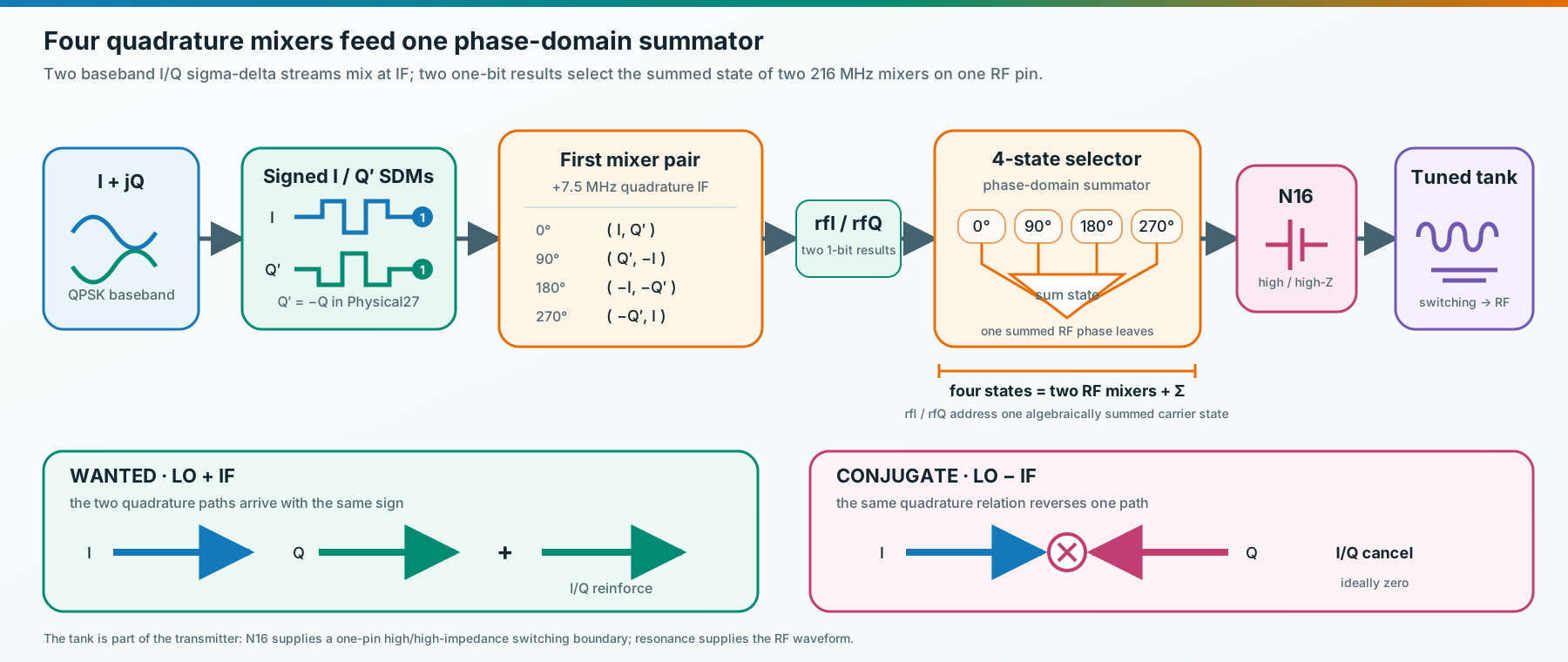
Four quadrature mixers and a phase-domain summator turn two baseband I/Q sigma-delta streams into QPSK on one FPGA output pin. N16 switches among four phases of a 216 MHz PLL clock and excites a hand-built resonant tank.
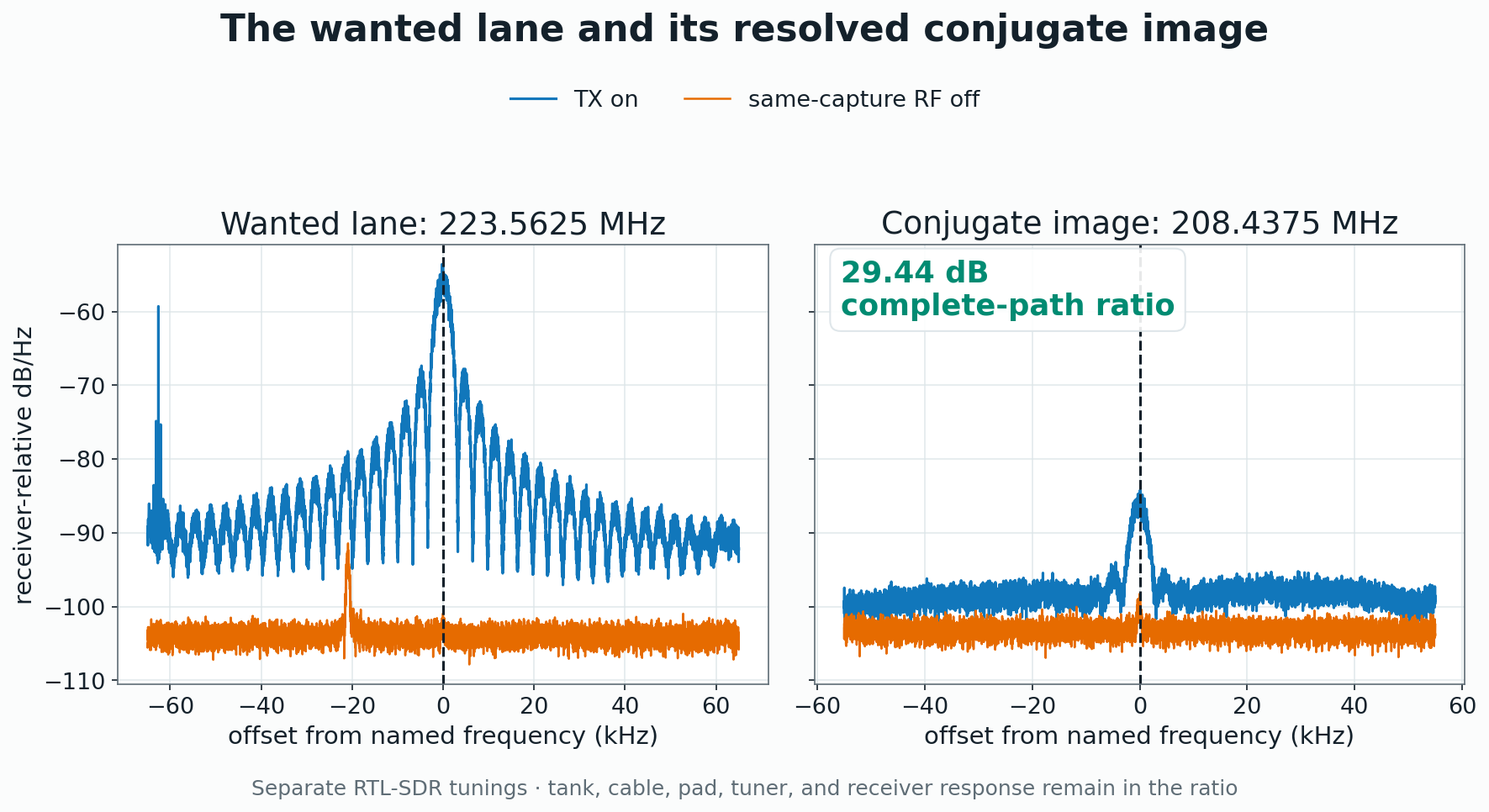
At the wanted frequency, I and Q reinforce; at the conjugate image, they oppose. On July 26, the complete tank-to-receiver path placed a 223.5625 MHz lane 29.44 dB above its 208.4375 MHz image. A 500 kHz upper-sideband run filled a rectangular spectrum with 1.14 dB of level spread across its flat core.
29.44 dBwanted / true image, complete path
35.2measured loaded tank Q
1.14 dB500 kHz flat-core spread
1 pinfinal programmable RF output
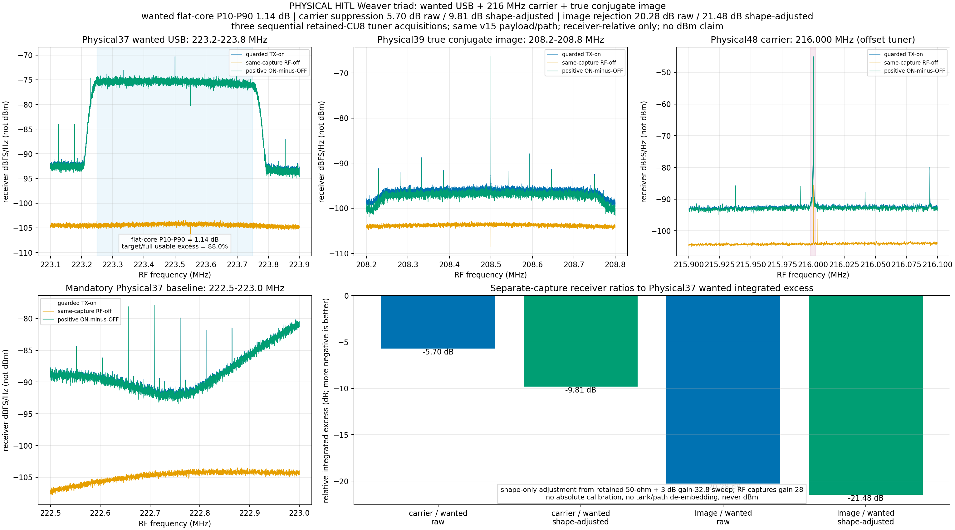
The July 26 Weaver triad: the square 223.25–223.75 MHz upper sideband, the 208.5 MHz true conjugate-image region, and the 216 MHz physical carrier. The wideband triad measured 20.28 dB of raw wanted/image separation; the narrow-lane pair below measured 29.44 dB. The receiver supplies relative levels. Download the plotted spectra.
Four Mixers Collapse Into One Four-State Output
A Weaver transmitter uses two quadrature mixer pairs. Physical27 sigma-delta encodes I and −Q into one bit each. A +7.5 MHz quadrant sequence performs the first pair through exact swaps and inversions of that two-bit word, producing two one-bit intermediate signals.
Those signals control a selector with four outputs: 0°, 90°, 180°, and 270° phases of the physical 216 MHz PLL clock. Each state already contains the algebraic result of the second mixer pair and their sum. N16 switches the selected phase high or high impedance into the tank.
Let Q′ denote the selected quadrature polarity; Physical27 uses Q′ = −Q. The first pair forms I1 = I·cos(IF) − Q′·sin(IF) and Q1 = I·sin(IF) + Q′·cos(IF). The summator then emits I1·cos(LO) − Q1·sin(LO). LO+IF terms reinforce while LO−IF terms cancel. Reversing Q′ selects the opposite sideband.
The active Physical27 path implements four quadrature mixers followed by a phase-domain summator. The final selector emits their summed state on one RF pin.
The April 2025 mod_apr20.sv used opposing sawtooth baseband sources, two one-bit sigma-delta streams, the same four-mixer Weaver structure, and the same phase-domain summator. Physical27 advances that architecture with FPGA-native PRBS16 QPSK while retaining two one-bit intermediates, four physical carrier phases, the high/high-impedance N16 boundary, and the resonant tank.
Removing One Pilot Dropped The Center By 23.41 dB
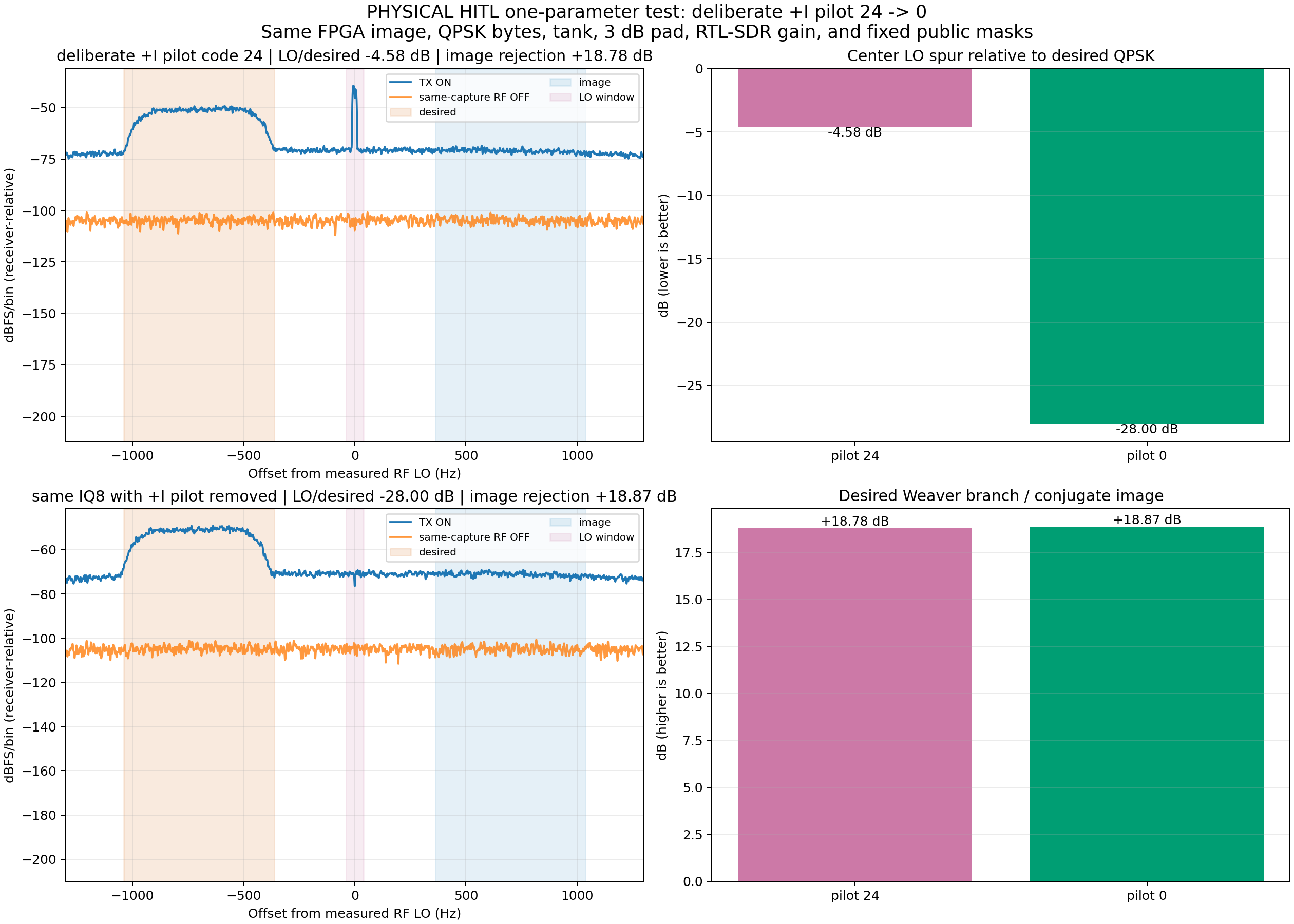
On July 25, a narrow QPSK upper branch crossed the FPGA, N16, tank, nominal 3 dB pad, and RTL-SDR. A deliberate +I pilot raised the translated center. Removing only that pilot dropped the center line by 23.41 dB while wanted power changed by 0.01 dB and the local opposite branch changed by 0.08 dB.
The pilot-free wanted branch stood 18.87 dB above the opposite branch and 28.00 dB above the translated center. Information occupied one side while both competing features fell away.
The same FPGA image, QPSK bytes, tank, pad, receiver gain, and fixed integration masks before and after pilot removal. The local opposite branch surrounds the translated center; the true RF conjugate image appears near 208 MHz. The receiver supplies relative levels. Download the measured ratios.
A 500 kHz Rectangular Sideband Filled The Tank
Physical37 streamed signed 16-bit I and Q at 750 ksample/s into the FPGA SDM/DDS/Weaver path. The tank-coupled output filled a 500 kHz upper-sideband core from 223.25 to 223.75 MHz with only 1.14 dB of P10-to-P90 level spread.
Sequential receiver tunings then captured the true 208.2–208.8 MHz conjugate image and the 216 MHz four-phase carrier. Raw integrated wanted/image separation reached 20.28 dB. The raw carrier sat 5.70 dB below the wanted band; coarse compensation for receiver shape placed the ratios at 21.48 and 9.81 dB.
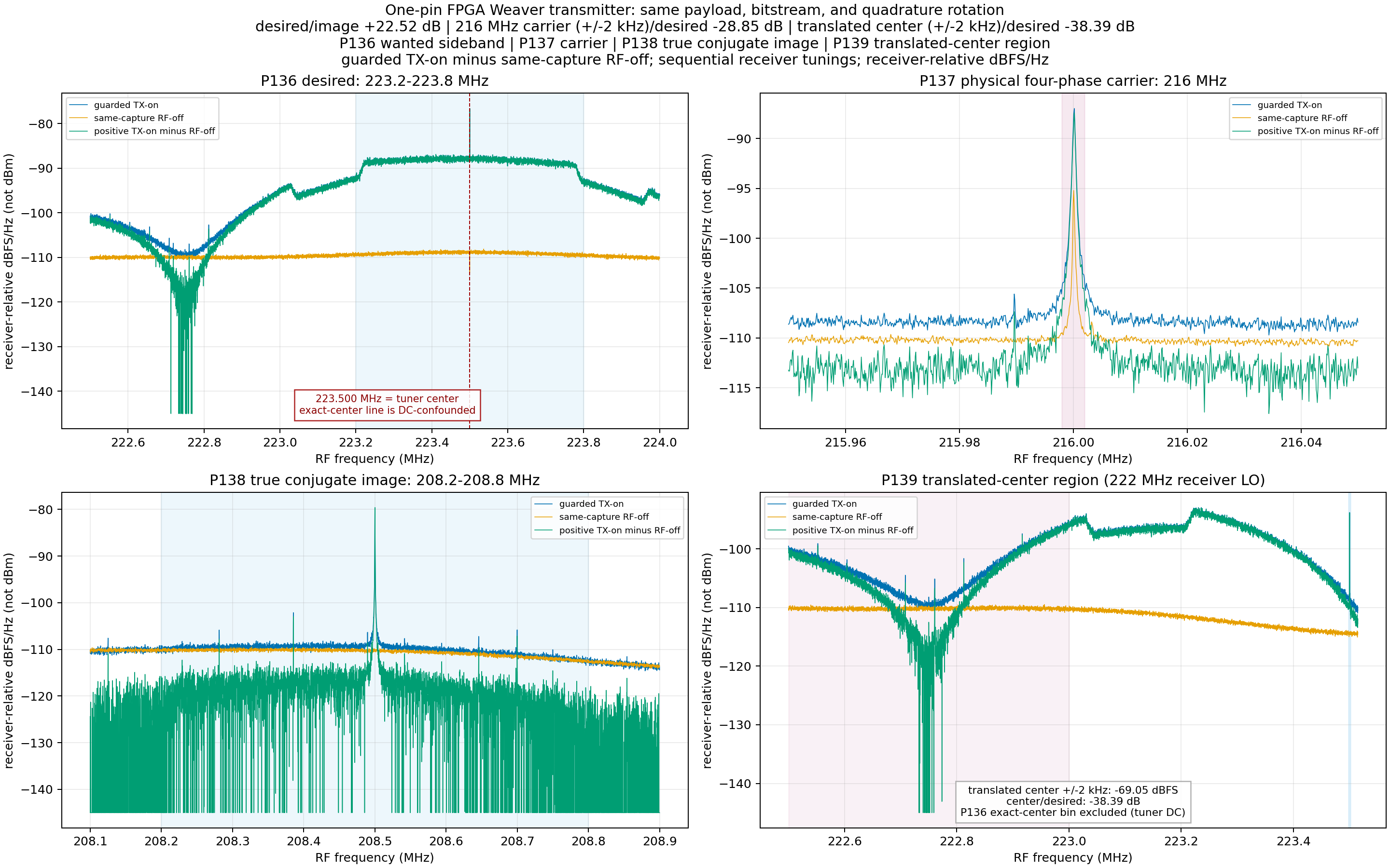
The three views above share the v15 payload and signal path, with one RF-off baseline per tuning. After midnight, a same-configuration four-view sweep tightened the 500 kHz flat-core spread to 0.929 dB, placed the carrier 28.85 dB below the desired band, placed a ±2 kHz translated-center window 38.39 dB below it while excluding the tuner-DC bin, and measured 22.52 dB desired/image separation.
Physical136–139, acquired from 1:12 to 1:17 a.m. PDT on July 27, share one payload, bitstream, rotation, and guarded acquisition sequence. The four sequential receiver tunings report relative levels. Download every plotted bin.
The Narrow Lane Beat Its True Image By 29.44 dB
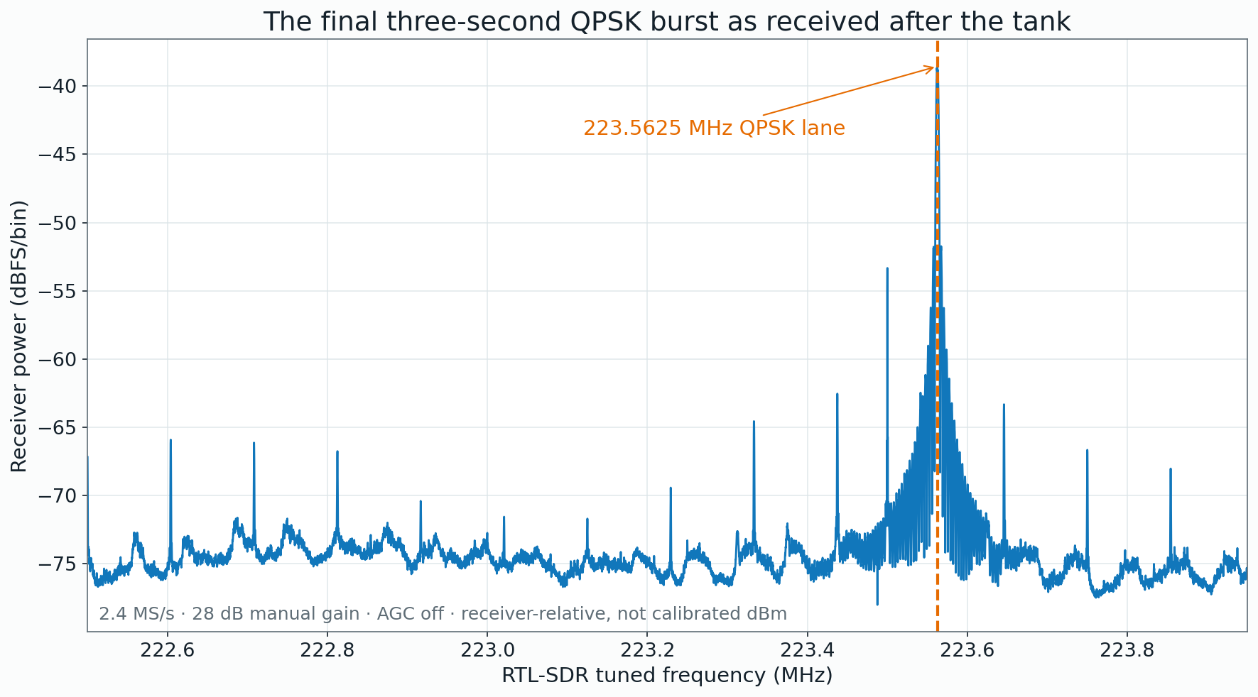
Physical27 sent an FPGA-native QPSK lane at 223.5625 MHz. Physical28 retained the FPGA image, gain, sample rate, cable path, and three-second gate, then moved only the RTL-SDR tuning to the predicted 208.4375 MHz conjugate image. Signed TX-on-minus-RF-off power in fixed 25 kHz windows produced a 29.44 dB wanted/image ratio.
Five broad NanoVNA sweeps measured S21 about 7.95 dB higher at 223.5625 MHz than at 208.4375 MHz, showing how the tank favored the wanted frequency. The NanoVNA and SDR used different instruments and reference planes: 7.95 dB describes tank transfer, while 29.44 dB describes the complete sequential transmitter-to-receiver path.
The wanted lane and its resolved true conjugate image. The sequential tank-to-receiver path measured 29.44 dB between them. Download the plotted windows.
The Tank Turns Timed Charge Into RF Power
The pMOS output injects timed charge into the coupled resonant network, then releases the pin. Electric and magnetic energy continue exchanging in the tank between FPGA edges. The phase sequence and tuned matter create the RF waveform together.
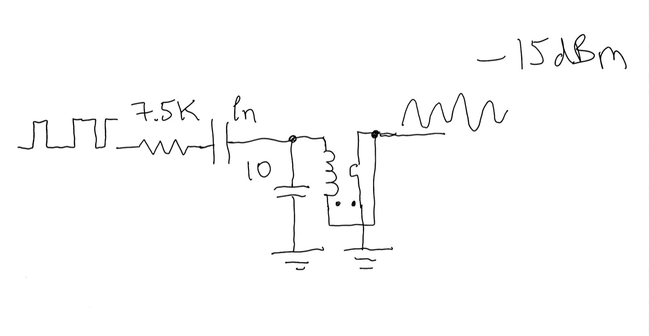
A historical bench sketch records about −15 dBm beside the earlier 7.5 kΩ coupling path. As a power unit, −15 dBm equals 31.6 µW; into 50 Ω, that equals 39.8 mV RMS or about 112 mV peak-to-peak for a sine wave. The sketch records the tank value without a load, output plane, bandwidth, cable correction, or instrument setup, so it remains distinct from the July 2026 receiver-relative measurements.
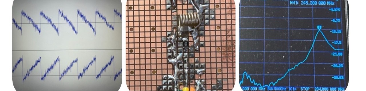
The original transmitter family: I/Q sawtooths, the coupled tank, and a historical analyzer view at 245.388 MHz. Each view records a separate part of the architecture.The contemporaneous topology sketch carries the rounded −15 dBm note and the earlier 7.5 kΩ value.
For the July 26 Physical27 run, the fixed 25 kHz wanted window integrated to −20.85 dB on the receiver analysis scale, and its peak reached −38.55 dBFS per FFT bin. Those values preserve the RTL-SDR's receiver-relative reference. An absolute-power pass can sample voltage at a named 50 Ω output plane and record the exact bitstream, tank load, carrier setting, probe factor, scope termination, and path loss together.
The Laboratory Closed One Causal Loop
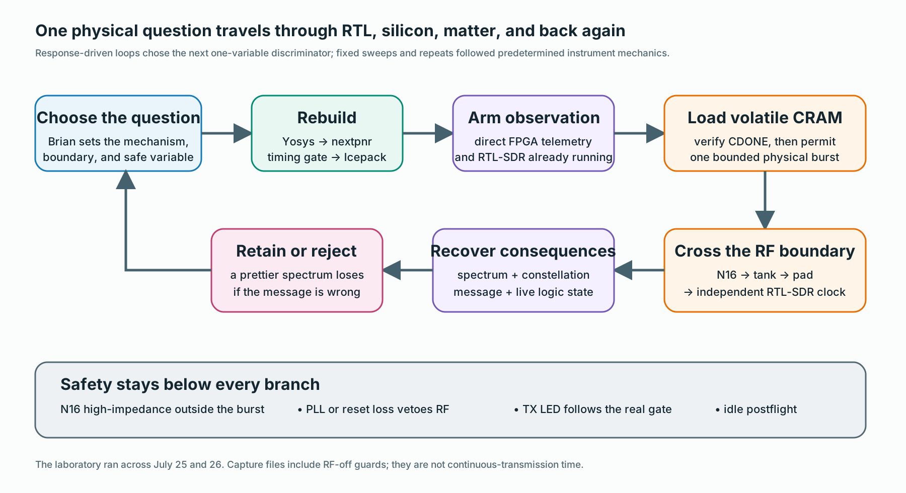
FPGA source, timing closure, volatile programming, live logic state, passive transfer, receiver tuning, RF-off baselines, packet recovery, and the next design decision all referred to the same physical event.
The run fixed the architecture, physical connections, 222–225 MHz operating band, and safety rules. Orchestration could then synthesize one variable, reject a timing failure, arm telemetry and the RTL-SDR before programming, load volatile CRAM, verify CDONE, capture one bounded burst, recover its received consequence, and return N16 to high impedance. Response-driven branches chose the next discriminator from the preceding physical result; predetermined sweeps and unchanged repeats handled instrument mechanics.
Each question crossed the complete path: design choice, timed FPGA image, live silicon state, resonant matter, received RF, recovered information, and the next physical question.
171RTL-SDR acquisitions
87configured NanoVNA sweeps
70volatile FPGA loads
42distinct FPGA images
Those counts span distinct instrument and programming operations across two calendar dates. Receiver captures include RF-off guard time. Most FPGA images emitted one finite burst and then returned N16 to electrical silence.
July 25: Ask The Physical Boundary One Question At A Time
The NanoVNA measured the passive network with the transmitter off. The RTL-SDR then measured the active path with the NanoVNA powered down. Early captures established tuner behavior, receiver gain, idle state, bounded on/off timing, harmonics within the receiver's usable range, and ADC headroom.
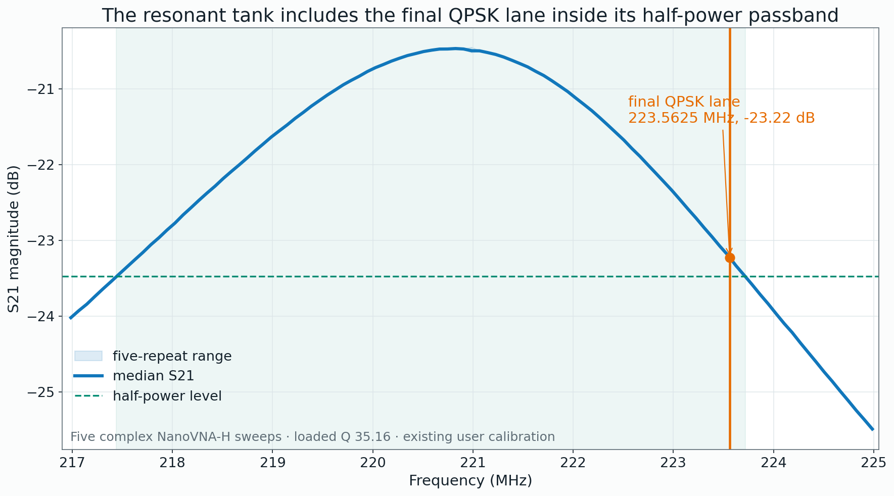
Five complex tank sweeps put the median S21 maximum at 220.783 MHz. The half-power crossings were 217.439 and 223.719 MHz, giving a 6.28 MHz loaded bandwidth and loaded Q of about 35.2. The later 223.5625 MHz QPSK lane lies about 156 kHz inside the upper half-power crossing. Its interpolated median S21 is about −23.22 dB, roughly 2.75 dB below the tank peak.
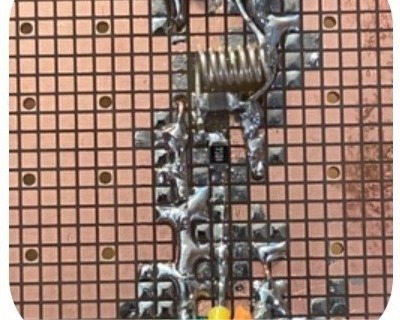
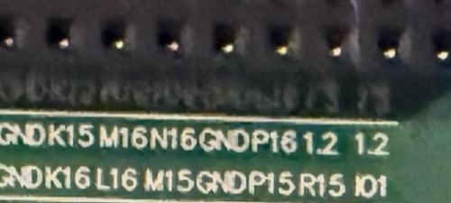
The hand-built resonant network used throughout the one-pin transmitter family.The board silkscreen around N16, the single programmable RF output pad.
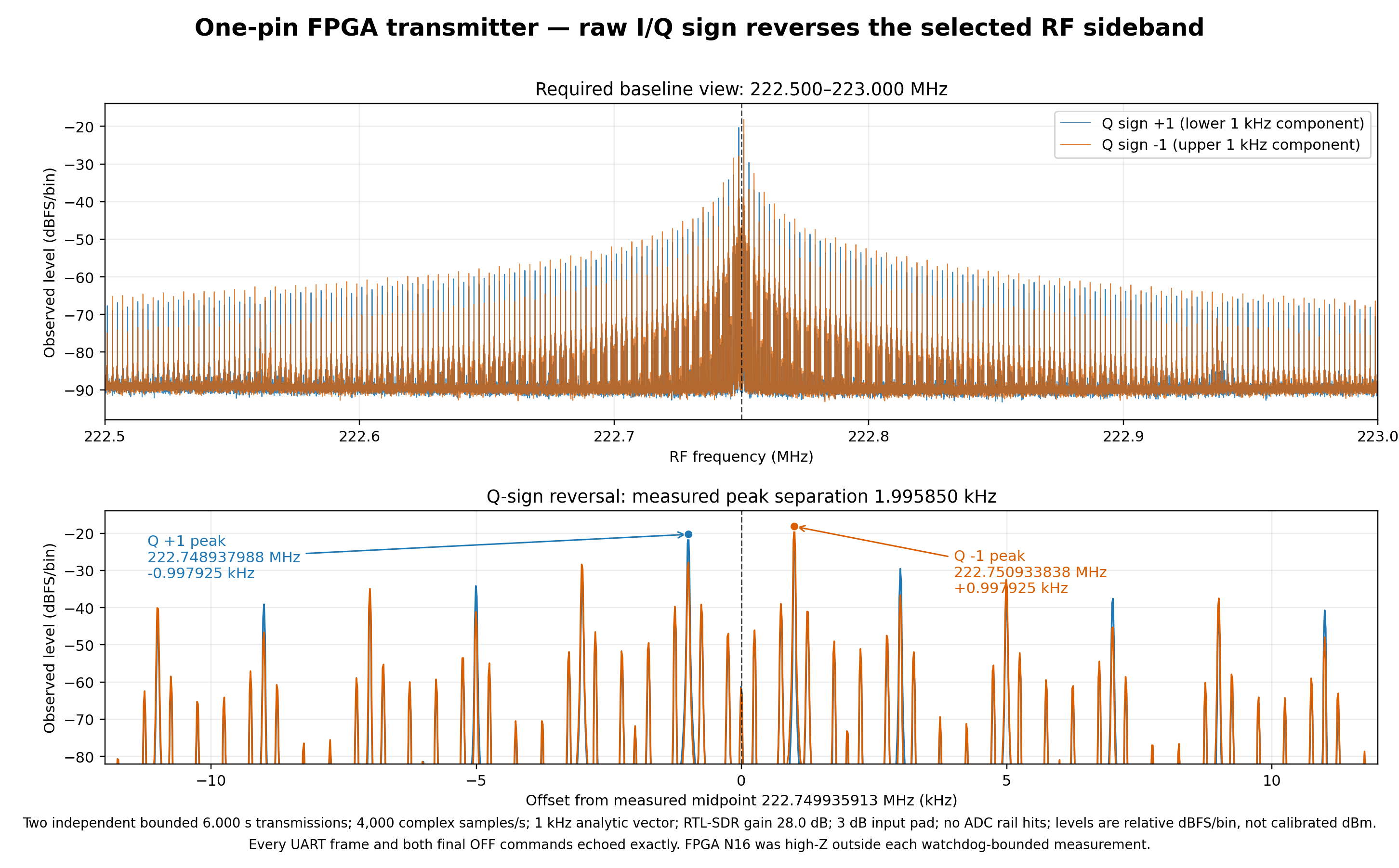
Changing only the sign of Q asked a clean causal question: would the physical RF component cross the carrier? The received peak moved from about −997.9 Hz to +997.9 Hz around the measured midpoint, a 1.996 kHz separation. The digital-to-physical boundary controlled direction as well as carrier gating.
Two bounded six-second transmissions across the full 222.5–223.0 MHz view and the close sideband view. Changing only Q's sign reversed the Weaver sideband. The receiver supplies relative levels. Download the plotted bins.
Separate Tunings Exposed Shape, Carrier, And Image
On July 26, three receiver tunings separated the wanted-band shape, residual 216 MHz carrier, and 208 MHz conjugate image. Each tuning exposed one observable, letting the next FPGA change address one mechanism.
July 25, 11:13
The board, tank, coupling path, receiver, and bounded operating sequence returned to service.
14:59–16:46
Q-sign reversal and pilot removal made the physical I/Q direction and translated-center suppression visible.
July 26, 16:48–17:50
Physical27 carried FPGA-native PRBS QPSK; Physical28 moved the receiver to the predicted true-image frequency.
20:57–21:23
Physical37 produced the 500 kHz square upper sideband; Physical39 and Physical48 added the true-image and 216 MHz carrier views.
July 27, 01:12–01:17
Physical136–139 repeated wanted, carrier, image, and translated-center views with one payload, bitstream, and rotation.
The FPGA Generated Its Own QPSK Payload
A PRBS16 generator inside Physical27 began from 0x1D2B, advanced with p15 ^ p13 ^ p12 ^ p10, and mapped lane 62 as {p5 ^ 1, p7}. Its four states carried 0=+I, 1=+Q, 2=−I, and 3=−Q.
The timing-closed HX8K image used 2,127 of 7,680 logic cells, one of two PLLs, no block RAM, three global buffers, and seven I/O cells. The 12, 30, 108, and 216.03 MHz domains all passed their declared timing constraints. A 324,000,000-cycle gate created one nominal three-second burst at 3,295.9 symbols/s and 6,591.8 gross bits/s.
The April 2025 mod_apr20.sv transmitter used opposing sawtooth baseband sources, two sigma-delta streams, a quadrature IF mixer pair, and the same phase-domain summator. V10 retains four mixers, two one-bit intermediate signals, the pMOS-only N16 boundary, and the external tank. FPGA-native PRBS QPSK, a complex lane waveform, signed SDMs, complete-word +7.5 MHz rotation, one-shot gating, and direct telemetry replace the earlier baseband and IF implementation.
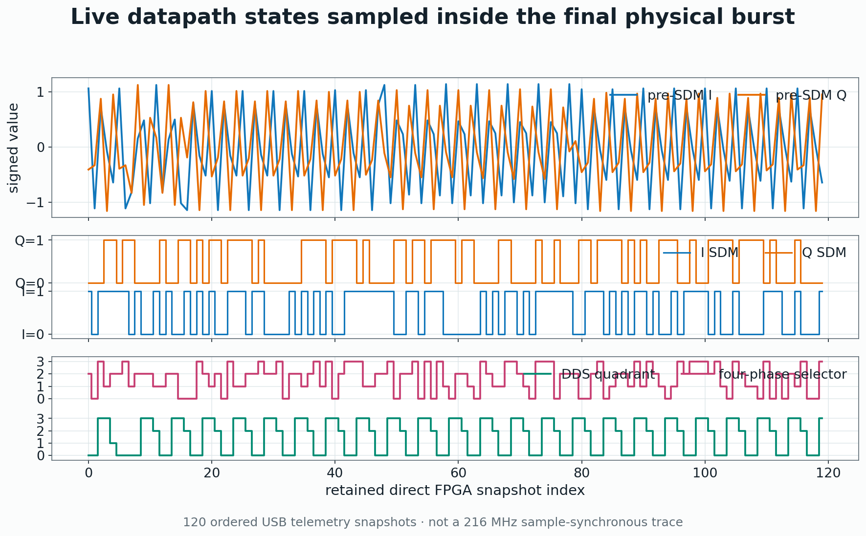
Ordered snapshots from the live v10 datapath: pre-SDM I/Q, both one-bit SDM outputs, first-mixer DDS quadrant, and phase-domain summator state. USB telemetry samples live states independently of the 216 MHz clock. Download the 120 plotted snapshots.
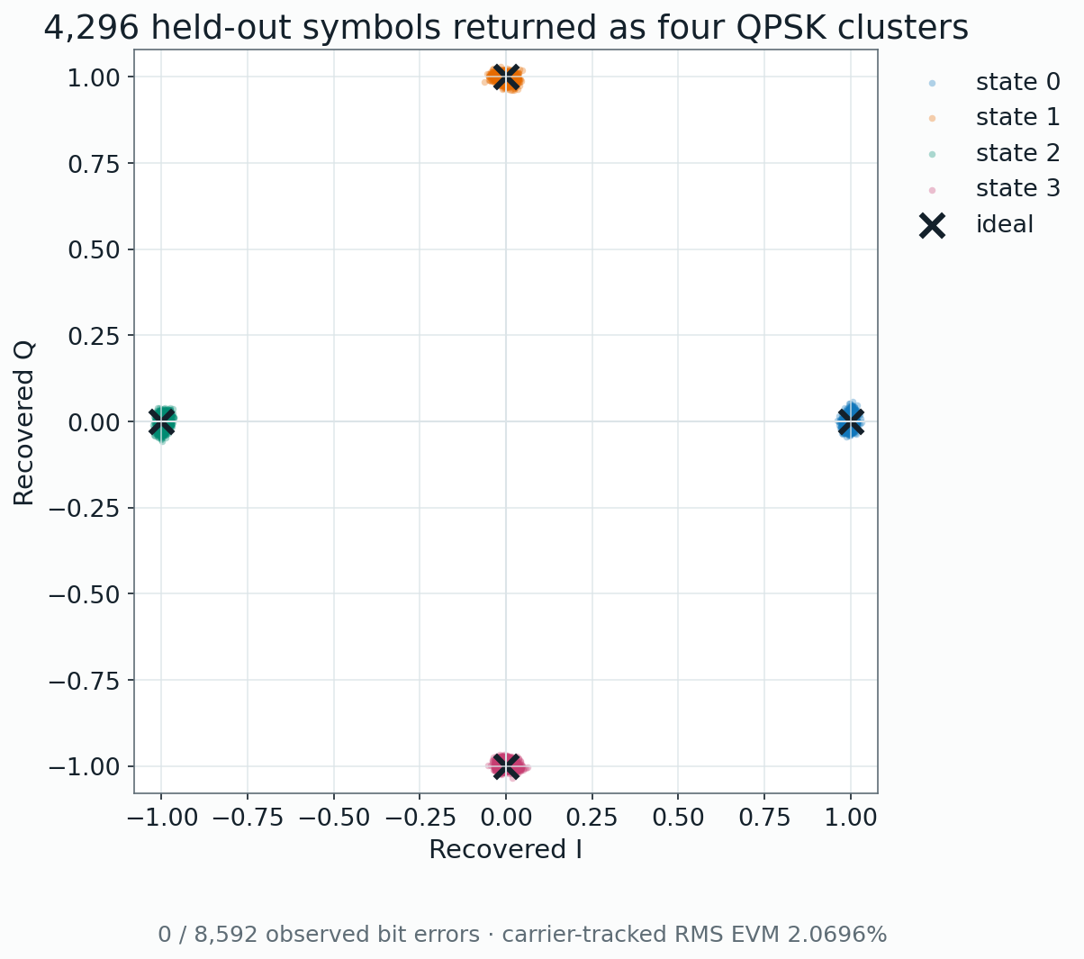
Physical27 armed the RTL-SDR and direct telemetry before programming the FPGA. The receiver captured unsigned 8-bit complex samples at 2.4 MS/s around 223.4875 MHz. Analysis mixed the 223.5625 MHz lane to baseband, averaged groups of 45 input samples, applied a 257-tap 10 kHz low-pass filter, and located one 3.008-second burst through channel energy alone.
A fourth-power carrier tracker learned its smoothing width from early directly observed epochs, then followed received I/Q during held-out data without consulting held-out truth or decisions. The early region fixed timing, orientation, clock scale, complex gain, and offset. Thirteen interpolated samples across the central 72% of each epoch produced every symbol.
The nominal held-out span contained 5,623 epochs. Direct telemetry reached 4,296; 1,327 holes remained absent. Across the complete run, 2,332 epochs lacked telemetry, and the scorer omitted them. The 4,296 observed symbols yielded 8,592 checked bits with zero errors in this burst, 2.07% carrier-tracked RMS EVM, and 0.9996 normalized correlation.
The bench operated inside an RF chamber. Every final profile used volatile configuration, defaulted N16 to high impedance, vetoed RF after PLL or reset loss, and drove the TX LED from the physical gate. Physical27 and Physical28 ended with N16 at high impedance, the burst inactive, and the TX LED off.
The chamber confined each transmission. A calibrated exterior field-strength sweep can add distance, antenna factor, orientation, detector, bandwidth, ambient baseline, uncertainty, and field units for regulatory work. These runs stayed inside the chamber and exercised system behavior rather than outdoor legal-power operation.
Listen To FM Cross The Same Physical Path
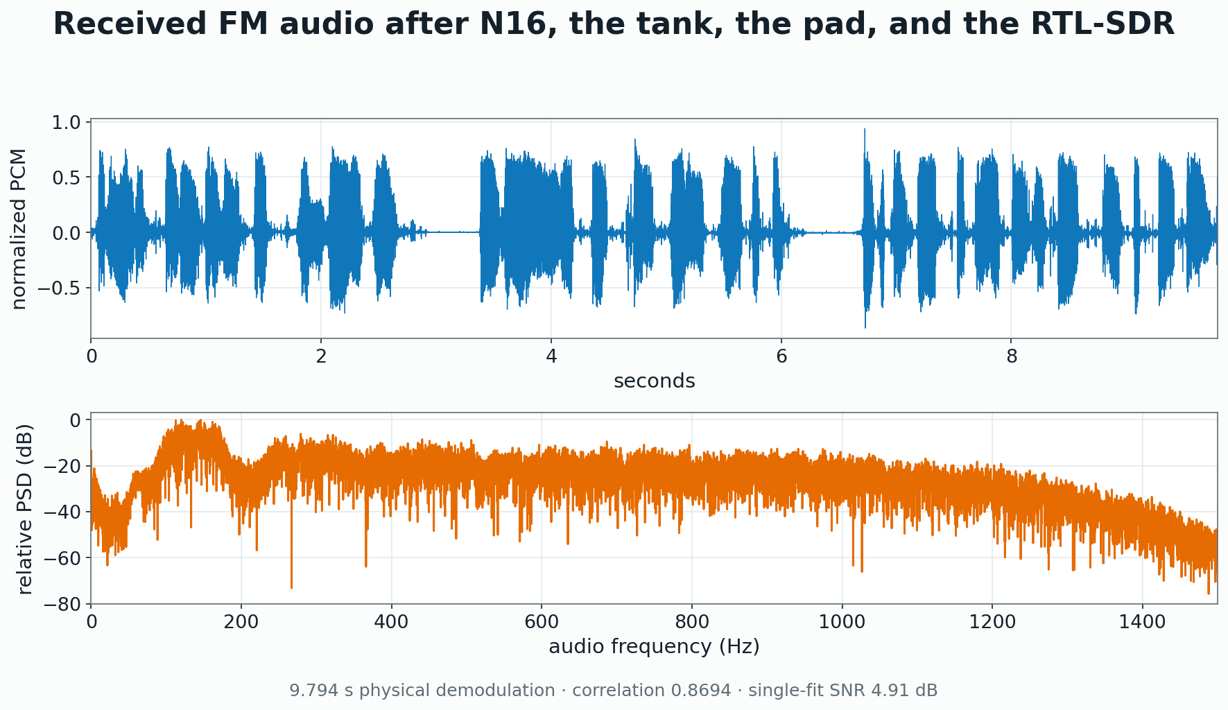
Before the FPGA-native PRBS run, a July 25 complex-FM image carried a privacy-neutral spoken report through N16, the tank, the nominal 3 dB pad, and the RTL-SDR. The physical demodulation lasts 9.79 seconds. Against its exact source-phase model, the longer fitted interval reached 0.869 correlation and 4.91 dB single-fit SNR, with a 56.8% EVM-like residual.
The recognizable audio records the earlier FM branch; Physical27 later replaced it with FPGA-native QPSK.
The public WAV contains the physical receiver demodulation. A clean RIFF container carries the audio without source metadata.
Extend The Same Loop Across A Wider Measurement Plane
Traceable conducted power, common-clock timing, repeatability, and additional operating modes can turn the working loop into a broader RF development platform.
The operating foundation
Bounded volatile FPGA images with high-impedance idle behavior.
Direct applied-symbol and live-datapath telemetry beside independent RF capture.
Repeatable passive tank transfer and same-capture RF-off baselines.
Response-driven one-variable experiments that can reject an attractive failure.
Finite FPGA-native QPSK recovery through the complete physical path.
Traceable measurement
Complete tank schematic, measured BOM, geometry, loading, cables, and named reference planes.
Raw TDS3034C waveform at the intended RF output plane, tied to the exact image, carrier setting, load, and scope configuration.
Traceable amplitude calibration and conducted output power with uncertainty.
Common-trigger or common-clock FPGA/RF timing instead of host-edge association.
Repeated bursts, temperature and supply monitoring, drift, and a real BER-versus-condition curve.
Wider laboratory control
Calibrated exterior chamber field-strength sweeps with distance, antenna factor, orientation, detector, bandwidths, ambient baseline, and uncertainty.
Final-profile harmonic and out-of-view emissions work with an instrument that can cover the required range.
Neutral public audio and packet reruns generated by the final FPGA-native datapath.
A browser control surface that can launch safe predetermined experiments and replay privacy-clean numerical traces.
Build And Score The V10 Transmitter
Run bash scripts/build-v10.sh to regenerate the v10 netlist, route report, and FPGA image. All four declared clocks pass timing. The bundle includes RTL, generated constants, constraints, the build script, route summary, scorer, and held-out points.
Brian publishes the source for study and reproduction and retains all reuse rights unless he grants a separate license.
Source tree
RTL, generated tables, constraints, build script, route summary, and a local scoring program.