Complete source package
All RTL, constraints, build and SRAM-load scripts, hardware notes, MIT terms, and the ready-to-load one-second image.
Download the ZIPOpen RF IP · iCE40HX8K · 106-channel complex synthesis
This is an entire frequency-agile transmitter fabric converging on one physical pin.
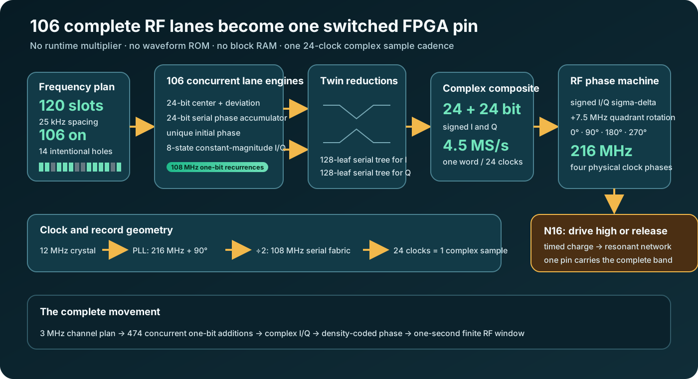
Brian Greenforest fit 106 independently phased, deterministically modulated FM lanes into one HX8K. They occupy a 120-slot grid from 222.0125 to 224.9875 MHz, preserve fourteen deliberate holes, and produce 4.5 million complete 24-bit I/Q samples per second. Two one-bit sigma-delta streams then drive a four-phase 216 MHz Weaver selector whose complete RF result leaves through N16.
No runtime multiplier, waveform ROM, block RAM, parallel bank of DAC pins, or external I/Q modulator creates the band. The channel plan, modulation, phase accumulation, complex addition, density conversion, frequency translation, finite transmit window, and live status are FPGA logic. The complete SystemVerilog and rebuild package are MIT licensed so you can change the mask, modulation family, channel spacing, burst length, output network, or product around it.
The startling part is not the channel count by itself. It is that all 106 channels are alive concurrently, each with its own 24-bit translation phase, deterministic initial phase, modulation identity, and true quadrature waveform, while the implementation spends only one bit of arithmetic width at each local recurrence.
A conventional reading of “106 channels” suggests 106 wide NCO adders, 106 sine tables, 212 multipliers for complex mixing, a broad parallel adder fabric, and a multi-bit DAC. This source builds a different machine. Twenty-four clocks are one arithmetic word. On each clock, every active lane advances one bit of its center-plus-deviation sum, one bit of its phase accumulation, and one bit of its I/Q contribution. The entire array keeps time together.
The design contains 474 concurrent one-bit addition recurrences: eight modulation accumulators, 106 center-plus-deviation adders, 106 per-lane phase accumulators, and 254 nodes in the twin I/Q reduction trees. Width becomes time without making the lanes take turns. That distinction is the magnitude: the arithmetic is serial inside every channel and spatial across all channels.
The channelizer's complex sample rate falls directly out of its serial word:
108,000,000 serial clocks/s ÷ 24 bits = 4,500,000 complex samples/s
Lane zero begins at −1.4875 MHz complex baseband. Lane 119 ends at +1.4875 MHz. The source advances by 25 kHz per lane with:
bin  = -119 + 2 × lane
tune = round(bin × 2^24 / 360)
The denominator 360 is the exact relationship between a 12.5 kHz half-step and the 4.5 MHz complex sample rate. The odd-valued bin sequence therefore lands at −1,487,500, −1,462,500, and onward through +1,487,500 Hz without a stored frequency table.
A common +7.5 MHz complex rotation moves that baseband around 223.5 MHz on the 216 MHz physical clock. The first and last centers become 222.0125 and 224.9875 MHz. The edges of their 25 kHz slots are exactly 222 and 225 MHz: one contiguous 3 MHz canvas.
CHANNEL_MASK is the plan. Its 106 one-bits instantiate active lane hardware; its fourteen zero-bits become deliberate holes. The active positions are:
Active: 0–1, 3–7, 11, 15–21, 23–26, 30–109, 113–119
Holes:  2, 8–10, 12–14, 22, 27–29, 110–112
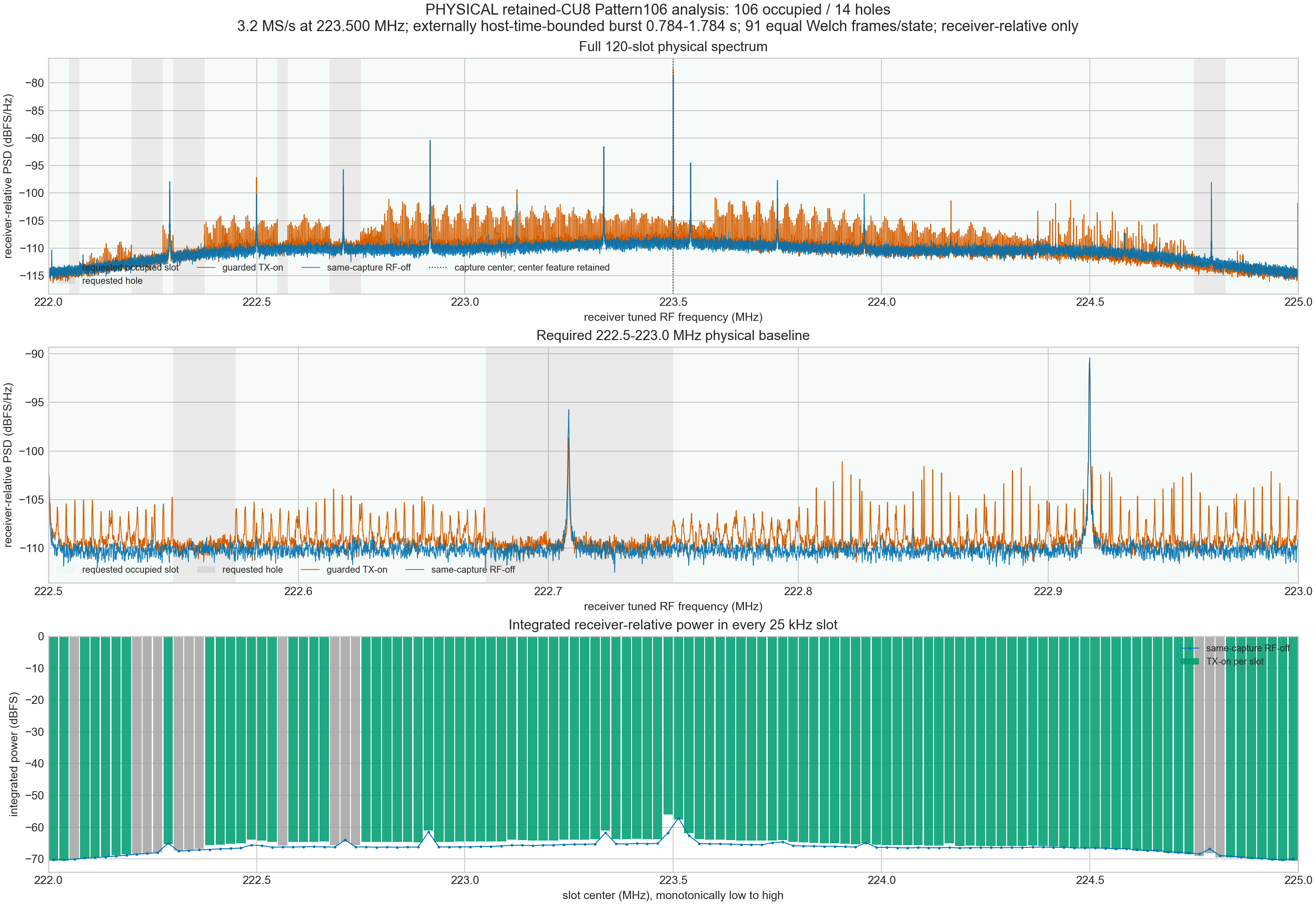
This is more powerful than muting samples after synthesis. The generate condition removes an inactive lane from the implemented transmitter. Change one mask constant and the physical array itself changes. The spectrum illustration's gray columns are those same fourteen source-level decisions carried all the way to the receiver view.
Each occupied lane begins with 0x123456 + lane × 0x9e3779, giving the grid a deterministic spread of starting phases. Two iCE40 LUTs serialize the lane's compile-time center word locally. An eight-way registered selector chooses the current deviation bit. One serial full adder forms center plus deviation; a second one-bit recurrence accumulates that tuning word into phase.
The carries clear at explicit word boundaries. tune_word_start, phase_word_start, and lane_word_start are intentionally offset by one clock each so the selector, tune addition, phase snapshot, and waveform bits arrive in causal order. Fifteen local 24-cycle counters each serve eight lanes, containing the frame-index fanout instead of stretching one chip-wide control net across the array.
Only the top three phase bits are needed for the emitted waveform. They select one of eight points around a complex octagon. That is enough angular resolution to create a true I/Q phasor while keeping the lane's output logic tiny.
The axial points are (±65,536, 0) and (0, ±65,536). The diagonal points are (±46,341, ±46,341), the integer form of the same radius at 45 degrees. Every lane therefore contributes the same intended complex magnitude while its phase moves around the octagon.
That amplitude is deliberately generous and safe. Even if all 106 lanes align on one Cartesian axis, the sum is 6,946,816. A signed 24-bit word reaches 8,388,607, leaving 1.638 dB of headroom. No limiter or wide post-sum scaling stage is needed.
The two lookup functions emit I and Q independently. They are not mirrored copies or a duplicated scalar stream. At 0 degrees the lane is +I; at 90 degrees it is +Q; the diagonal states carry both components with the correct signs. Complex direction exists before the lanes ever meet.
Eight shared 24-bit modulation accumulators use signed step magnitudes 17, 23, 29, 35, 41, 47, 53, and 59. At 4.5 million updates per second, their fundamental cycles span 4.5598 through 15.8251 Hz. Four three-bit slices reuse those phase streams at 1×, 2×, 4×, and 8× rates, extending the profile cycles through 126.6003 Hz.
The lane number itself selects a unique tuple:
bank       = lane mod 8
rate slice = floor(lane / 8) mod 4
profile    = floor(lane / 32)
Profile zero passes the selected three-bit bank state directly; profile one complements it. The modulation accumulator direction alternates with bank parity, so both mappings carry forward and reverse motion across the lane set. Profile two traverses a triangle. In profile three, even lanes follow an eight-state sine-shaped path and odd lanes combine two phase banks. Initial phases add another deterministic separation.
All profiles share eight instantaneous tuning offsets from −45,000 through +45,000 phase-word units. At 4.5 MS/s that is ±12,069.940567 Hz: 24,139.881134 Hz from minimum to maximum inside each 25 kHz slot, with 860.118866 Hz between neighboring instantaneous ranges. The result is a deliberately dense wall of individually moving FM lanes, not 106 copies of one oscillator state.
Every active lane emits one current I bit and one current Q bit. Those 212 bits enter two balanced binary trees. Each tree has 128 leaves and seven registered levels: 64 adders, then 32, 16, 8, 4, 2, and 1. That is 127 serial additions for I and another 127 for Q.
The word-start pulse is delayed one register per level, so each one-bit full adder knows exactly when to discard the previous word's carry. Tree depth changes latency, not cadence. After the pipeline fills, the roots emit one I bit and one Q bit on every 108 MHz clock.
The output registers rebuild those roots into two signed 24-bit words. Every twenty-fourth bit raises a strobe, toggles the sample marker, and increments the serial-word epoch. One new complex composite therefore appears at 4.5 MS/s continuously.
This is the same Greenforest serial-arithmetic principle used by the continuous 64-bit multiplier, expanded here into a complete radio array: thousands of local state transitions produce wide mathematical behavior without carrying a wide result bus through every stage.
The 24-bit composite I and Q values feed two first-order signed sigma-delta loops at 108 MHz. Each loop keeps a 26-bit error state, compares its sign, emits one bit, and feeds back either +223 or −223. Pulse density now carries the signed component value.
Q is negated before conversion to choose the desired complex translation direction. The two resulting bits are not yet the RF output. Together they are a four-state complex word: the instantaneous sign choice for I and Q. The next stage rotates that complete word rather than mixing the components through separate multiplier chains.
The Gray-quadrant DDS advances by five in a modulo-144 phase space on every 216 MHz clock:
216 MHz × 5 / 144 = 7.5 MHz
Four phase regions transform (I,Q) into (I,Q), (Q,−I), (−I,−Q), and (−Q,I). That is a table-free complex rotation. The pair coming out of the DDS addresses four physical PLL phases: 0, 90, 180, and 270 degrees of the 216 MHz clock.
The selector is the Weaver sum in phase form. Its selected clock phase already embodies the two component mixes and their algebraic combination. The original one-pin quadrature transmitter develops that phase-domain sum from first principles; the QPSK signal-path article follows the same four-phase boundary from complex bits to N16.
The final SB_IO has constant data input one. The modulated RF bit controls output enable. A selected interval drives N16 high; the complementary interval returns it to high impedance. The pin never has to force the resonant node low.
N16 feeds a coupling path and magnetically coupled resonant network. Each enabled edge contributes timed charge. Between edges, electric and magnetic energy continue exchanging in the tank. Digital phase selection determines when energy arrives; resonant matter determines how that energy persists and emerges as RF. The FPGA and tank are one transmitter mechanism.
That is why one pin can carry a complete 3 MHz complex band. It is not imitating a 48-bit parallel DAC interface. It is controlling the phase and timing of physical energy directly.
The top-level parameter RF_COMPILE_ARMED defaults to zero. An armed build still waits for synchronized PLL lock, a 256-cycle startup interval, and channelizer readiness. Only then does gf_one_shot_burst_gate permit N16 to switch.
The standard window is 108,000,000 cycles at 108 MHz: exactly one second. During that interval the channelizer delivers 4,500,000 complete complex samples. When the counter expires, burst_done remains asserted and N16 remains high impedance until the FPGA is configured again.
The red LED derives from the same transmit window. A coherent 16-byte MPSSE frame reports PLL lock, reset, readiness, active/done state, outputs-off state, activity, consumed sample count, serial epoch, profile B5, configuration epoch 7, and the active-channel count. The transmitter operates autonomously; telemetry lets an instrument host watch the silicon without becoming part of the RF datapath.
The top panel spans all 120 slots from 222 to 225 MHz. It overlays the guarded RF-on interval in orange with the RF-off intervals from the same receiver acquisition in blue. The dotted 223.5 MHz line marks the common translation center; the center response is retained rather than erased.
The middle panel opens the required 222.5–223.0 MHz region. It makes the dense comb-like modulation structure and selected gray hole groups easier to see. Both traces use 91 equal Welch frames per state, so the visual comparison is formed from matching amounts of receiver time.
The bottom panel integrates receiver-relative power in every 25 kHz slot. Green bars name the 106 positions requested by the HDL mask; gray regions name the fourteen holes. Because the slots are ordered monotonically from low to high frequency, the physical picture can be read directly against the lane number and CHANNEL_MASK in the source.
gf_signed_sdm24_lean: signed 24-bit sample to one-bit density streamif (1'b0); it produces no implemented hardwareg_lane_ring: the active 106-lane center serializer, deviation selector, serial tune adder, NCO, and I/Q generatorThe synthesis closure adds two compact files. gf_pattern106_support.sv supplies the serial adder, one-shot gate, quadrant DDS, and four-phase selector. gf_mpsse_snapshot16_lean.sv supplies the cross-clock coherent telemetry frame. There are no hidden generated HDL files behind the top.
The build explicitly rejects runtime multiplication and block-RAM inference. The capacity goes into lane state, serial arithmetic, local timing, registered reduction, and the physical phase path. The clean public source rebuild produces the same ready-to-load FPGA image used for the spectrum above.
All RTL, constraints, build and SRAM-load scripts, hardware notes, MIT terms, and the ready-to-load one-second image.
Download the ZIPOpen the complete channel plan, 106 active lane generators, serial trees, SDMs, clocking, burst gate, and N16 boundary.
Read the SystemVerilogInstall Yosys, nextpnr-ice40, and IceStorm; build armed or high-impedance; load volatile SRAM; connect the switched output correctly.
Open README.mdLoad the one-second Pattern106 image into volatile HX8K SRAM with the included iceprog -S helper.
Exact CT256 pins for the 12 MHz crystal, N16, LED, and FT2232H channel-B telemetry, plus all clock declarations.
Open the PCFUse, copy, modify, merge, publish, distribute, sublicense, and sell copies. Keep the copyright and permission notice.
Read the licenseAfter extraction, the complete armed build is one command:
RF_COMPILE_ARMED=1 BURST_CYCLES_108=108000000 bash ./build.sh
Then load volatile SRAM:
bash ./program_sram.sh build/pattern106_iq24_lean_mpsse_v3.bin
Change CHANNEL_MASK for a new spectral stencil, then update the telemetry frame's active-channel-count byte to match. Change the lane tuning equation for a different grid. Replace the deterministic profiles with your modulation. Retarget the phase selector or output network. The architecture is public precisely so the next transmitter does not have to begin from a black box.
This source makes a 106-channel RF canvas available as ordinary editable logic. It can become a channel emulator, compact signal source, multi-tone instrument, deterministic interferer for a shielded bench, coded beacon family, test-vector generator, or the frequency fabric inside a larger radio system.
If you want Brian to adapt this architecture to another band, FPGA, channel plan, waveform family, instrument, product, or research program, start the conversation. Bring the spectrum you want to own and the physical boundary it must cross.