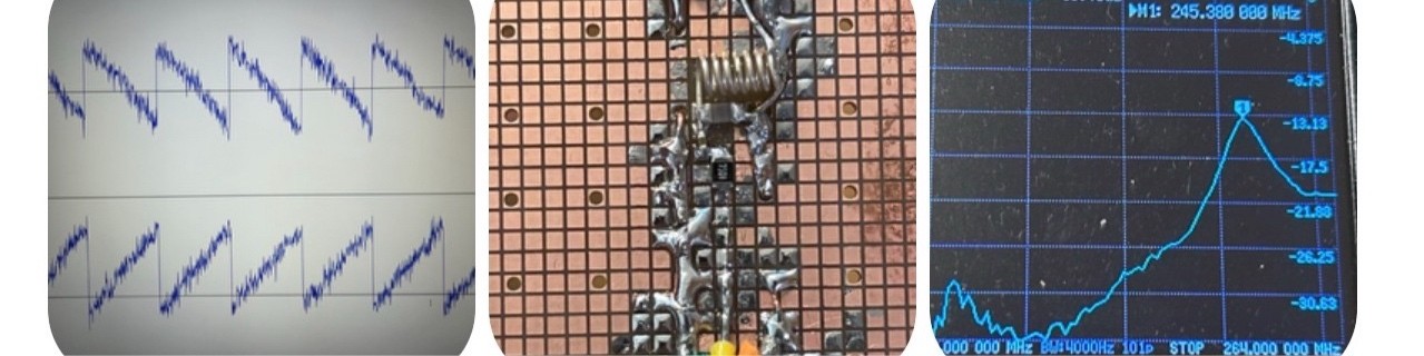
Four Mixers Become One Selectable Phase
The April 2025 transmitter is in one-pin-RF/ptc_nov21/mod_apr20.sv. The adjacent build script, HX8K constraints, and nextpnr timing declarations use the open Yosys, nextpnr, IceStorm, and iceprog path.
Opposing 32-bit sawtooths create complex baseband motion, and two sigma-delta paths reduce I and Q to one bit each. A Johnson counter supplies the quadrature IF oscillator; adjacent taps drive the first mixer pair. The complete quadrature relationship rejects the conjugate image, and the resulting rfI/rfQ pair controls the selector that performs the phase-domain sum.
The Phase-Domain Summator Realizes Two 216 MHz Mixers and Their Sum
The source names two PLL outputs pll_216mhz and pll_216mhz_90. Their complements supply the other two phases. The four selector states encode every possible algebraic result of the two quadrature carrier mixers:
wire p1 =  pll_216mhz;
wire p2 =  pll_216mhz_90;
wire p3 = ~pll_216mhz;
wire p4 = ~pll_216mhz_90;

assign MODULATED_RF_OUT = rfI ? (
  rfQ ? p1 : p4
) : (
  rfQ ? p2 : p3
);
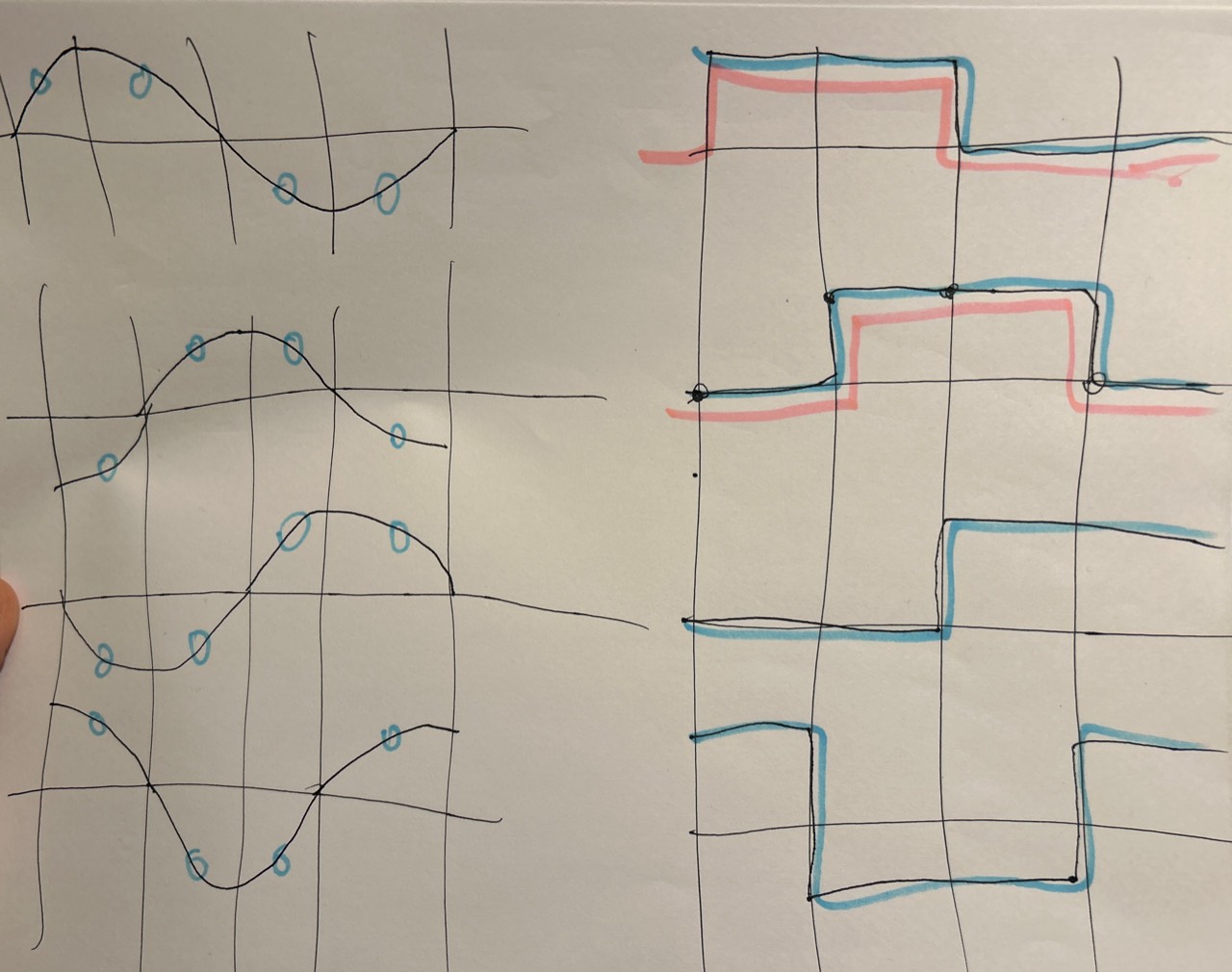
Each rfI/rfQ combination chooses the carrier phase equal to the sum of those two mixer products. The selector is therefore a phase-domain summator: it realizes the second mixer pair and their sum without two analog RF outputs or a downstream summer.
The First Mixer Pair Produces rfI and rfQ
Two sawtooth states move in opposite directions. Each feeds a one-bit sigma-delta path, producing dac_out and dac_outQ. Adjacent quadrature IF phases mix with those streams to produce the two one-bit intermediate signals.
sawtooth  <= sawtooth  - 32'd148000;
sawtoothQ <= sawtoothQ + 32'd148000;

wire rfI = dac_out  ^ j_0[0];
wire rfQ = dac_outQ ^ j_0[1];
The first two mixers create rfI and rfQ; those bits control the four-state selector that realizes the second two mixers and performs their phase-domain sum. Image rejection comes from that complete quadrature relationship: the wanted products reinforce while the conjugate products oppose.
N16 Becomes The Physical Summation Point
The HX8K CT256 constraint file maps RF_OUT to N16. Instead of an ordinary push-pull data assignment, an SB_IO primitive holds the data side high and applies MODULATED_RF_OUT to OUTPUT_ENABLE, using the pMOS side as the RF switch.
SB_IO #(
  .PIN_TYPE(6'b101000),
  .IO_STANDARD("SB_LVCMOS"),
  .PULLUP(1'b0)
) ddr_io_1 (
  .PACKAGE_PIN(RF_OUT),
  .D_OUT_0(1'b1),
  .OUTPUT_ENABLE(MODULATED_RF_OUT)
);
The FPGA chooses the phase at N16; the external network stores energy and turns those switched edges into narrowband electrical behavior.
The Resonant Tank Turns Edges Into RF
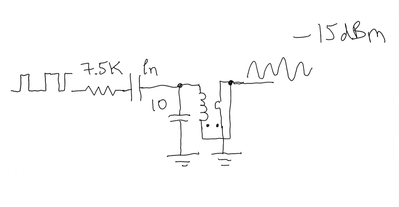
A phase-switched digital pin produces edges and harmonics. The tank stores field energy between those edges, favors the intended RF region, and couples a sinusoidal output from its secondary. The historical sketch shows a 7.5 kΩ coupling value; the July 2026 fixture uses a nominal 8.5 kΩ value and measures a loaded tank Q of about 35.2.
The Receiver Shows The Local Signal Beside Live Radio
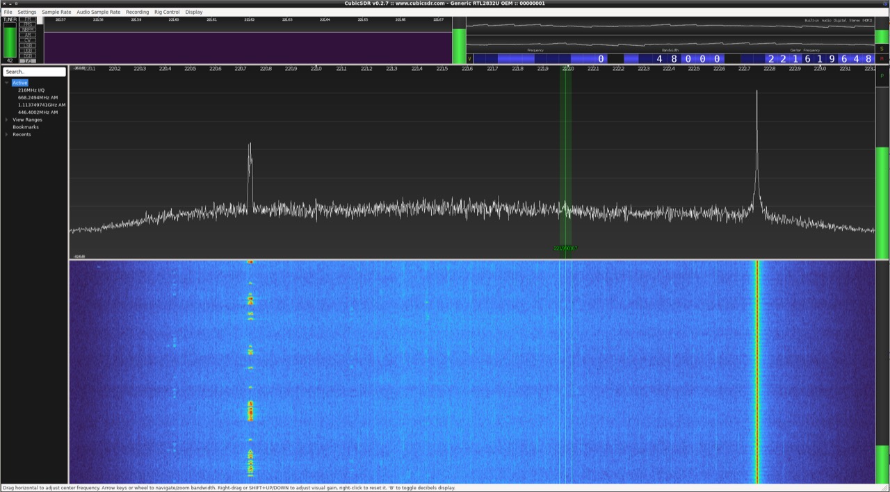
The local signal carries the expected sawtooth-like spectral shape beside the live channel. The 2026 continuation adds RF-off subtraction, fixed receiver windows, measured tank transfer, and separate views of the wanted band, 216 MHz carrier, and 208 MHz true image.
Why This Transmitter Matters
The design compresses four quadrature mixers and their final sum into FPGA primitives and one physical output: two one-bit intermediate signals, four carrier phases, one phase-domain summator, one switched pin, and one resonant network.
It creates a direct route from digital modulation state to RF phase and removes the conventional external I/Q modulator between the FPGA and tuned output network. That opens compact transmitter paths whose signal architecture lives almost entirely in reprogrammable logic.