The Missing Manufacturing Move
Claytronics asked for catoms: small units with computation, communication, actuation, adhesion, and collective behavior. The original CMU/Intel Research Pittsburgh framing already contained the crucial simplification: each unit should include only enough functionality to contribute to the ensemble.
That principle still feels right. A catom should not be a complete robot in miniature if the ensemble can supply power, clock, data, redundancy, mechanical structure, and control. The chiplet should be small because small parts can be manufactured, tested, sorted, and repeated. The ensemble should be intelligent because the individual particle should not carry the whole architecture alone.
The manufacturing move I care about is therefore not exotic atom-by-atom construction. It is closer to this: fabricate many active die on a normal wafer, dice them into small chiplets, passivate or coat them so they can survive handling and contact, then let adjacent chiplets exchange power, clock, data, and mechanical force through engineered near-field interfaces.
What The Wafer-Dicing Paper Contributes
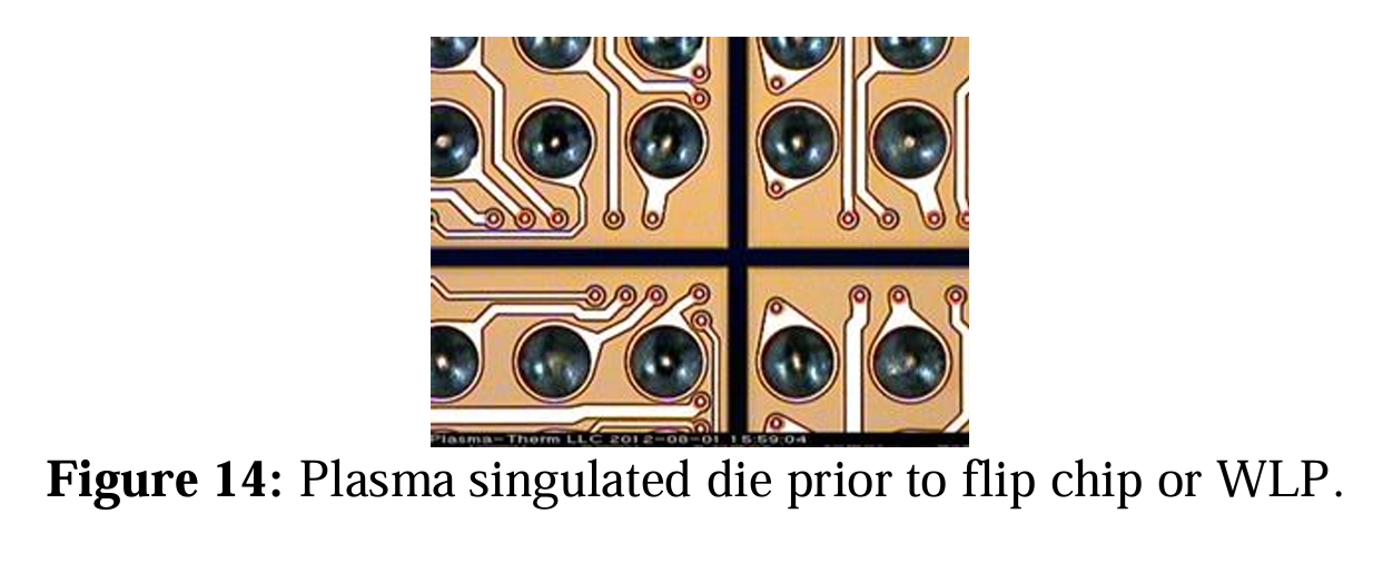
The dry-etch wafer-dicing paper is not a smart-dust paper. It is more valuable than that here: it shows that through-wafer singulation can be treated as a serious manufacturing step, not as a fantasy process attached to programmable matter.
The paper describes front-side plasma singulation on standard dicing tape and frames. It uses lithographically defined streets, reports typical singulation-line widths of 10-15µm, avoids some saw and laser damage mechanisms, and supports non-orthogonal or nonlinear dicing paths. In one test-wafer case, the authors report 10 to 15 percent more die per wafer.
Read narrowly, that is a packaging/process improvement. Read as a substrate clue, it says something stronger: if the active circuit is already on the wafer, then the particle boundary can be a designed geometric object rather than only a saw street. The chiplet can be shaped, protected, contacted, and repeated at wafer scale.
The Protected Chiplet
The candidate particle is not bare silicon dust. Bare die are fragile, electrically exposed, and mechanically hostile. The more interesting object is a tiny active chiplet with a dielectric skin, probably involving SiO2 or another passivation stack, and with deliberate capacitive, inductive, optical, or contact windows where the particle is supposed to couple to neighbors.
That coating is not decoration. It is the difference between a die fragment and a body. It protects the active island, defines the allowed electrical fields, sets the mechanical surface, and makes neighbor-to-neighbor interfaces more reproducible. If the skin is designed with coupling regions, then electrostatic or electromagnetic attraction can occur while power, clock, and data are also being transferred.
The hard part is co-design. The shape, coating, pads, resonators, interconnect, local storage, charge limits, thermal path, and test strategy have to be one object. If any layer is treated as an afterthought, the system becomes dust in the bad sense: tiny parts nobody can reliably power, address, cool, or recover.
Power, Clock, Data, And Force Should Share The Boundary
The old mistake is to imagine each particle as a sealed autonomous machine. That makes every chiplet carry too much: battery, radio, clock, processor, actuator, sensor, and failure management. It turns manufacturability into a miracle.
The ensemble approach suggests the opposite. Neighboring chiplets should use the same physical adjacency for several functions. Electrostatic or electromagnetic attraction can hold or move local structure. Capacitive or inductive coupling can move bits and timing. Resonant elements can store and redistribute energy across a region. The particle becomes less like a lone robot and more like a powered cell in a live fabric.
Resonant distributed energy storage is the key idea I do not want to lose. A large region of programmable matter cannot depend on every particle owning a private energy source. The region needs a way to guarantee that computation and actuation are powered as a field property: energy enters through accessible boundaries, sloshes through tuned local stores, and remains available to large connected subregions even while geometry changes.
Where Cartilage Fits
Cartilage matters here because programmable matter needs a model of computation that is native to space. A CPU-style program can control an array from outside, but that keeps the important structure hidden in a global controller. Claytronics needs computation that can live in the material: local state, local ports, local ownership, visible boundaries, repairable regions, and hierarchical reconfiguration.
That is exactly the architectural pressure behind Cartilage. The browser artifacts on this site are small, but the idea is not small: a region can own child regions, expose ports, accept configuration streams, and change its internal fabric while the boundary remains inspectable. That is the kind of computation model a programmable-matter substrate would need if macroscopic instructions are supposed to reach microscopic structure without becoming a single opaque broadcast.
This does not mean Cartilage proves Claytronics hardware. It means Cartilage supplies a missing language for the hardware: how to describe ownership, reconfiguration, routing, local repair, and nested scale without pretending that a global CPU is the material.
Why This Is Not Science Fiction In The Usual Sense
The speculative part is the integrated system. The non-speculative ingredients are more ordinary: wafers, passivation, dicing, chiplets, capacitive coupling, inductive coupling, resonators, clocks, local logic, error correction, and distributed protocols. None of those words require a new law of physics.
The question is whether they can be composed into a manufacturable substrate whose unit economics and physical behavior match the programmable-matter problem. That is different from saying the future is guaranteed. It is a better kind of question because it can fail in concrete places: yield, coating defects, alignment, adhesion, inter-particle communication, heat, ESD, radiation, charging, aggregate mechanics, and test coverage.
If this fails, I want to know where it fails. If it works even partially, then smart dust stops being only a science-fiction phrase and becomes a wafer-level packaging and distributed-systems problem.
Space Is The Most Serious And Most Dangerous Use Case
A cloud of resilient programmable chiplets in low Earth orbit is an obvious dream and an obvious warning. It could provide distributed solar power collection, compute, communications, sensing, inspection, and nanosatellite-style persistence without relying on a few large fragile spacecraft. It could also become surveillance infrastructure, debris risk, orbital clutter, or dual-use military hardware.
That dual-use fact should be stated early, not hidden behind optimism. Any path toward orbital programmable matter would need deorbit plans, identification, tracking, containment, radiation behavior, collision analysis, licensing, and rules for offensive and defensive use. A system that can compute, move, sense, and reconfigure in orbit is not politically neutral.
The reason I still care is that the same properties that make this dangerous also make it valuable: redundancy, radiation resilience, repair through reconfiguration, graceful degradation, and the ability to keep computation alive when individual pieces fail.
The Longest Claim
The longest claim is not that wafer dicing alone gives programmable matter. It does not.
The claim is that modern manufacturing may already contain enough of the physical toolkit to begin: wafer-scale active devices, small-die singulation, dielectric protection, near-field coupling, and distributed energy. Cartilage is my attempt to supply the matching computation toolkit: hierarchical spatial ownership, local reconfiguration, visible ports, and computation that remains inspectable as it scales.
If those two toolkits meet, then the path to programmable matter stops looking like a single impossible invention. It becomes a sequence of hard but nameable interfaces.
Open Questions
Observed: wafer-level semiconductor processes and plasma/dry singulation exist; the dicing reference shows through-wafer separation on standard tape and frames.
Implemented elsewhere: chiplets, passivation, capacitive links, inductive links, resonant power transfer, distributed algorithms, and microrobotics all exist in partial forms.
Argued here: a protected, wafer-diced chiplet could be a plausible catom substrate if its boundary carries mechanical, power, clock, and data roles together.
Speculative: large programmable-matter regions, self-repairing orbital compute, self-replication, atomic-scale scanning, and nanoscale fabrication loops remain unproved.
What I Would Value From A Reader
If you know wafer-level packaging, plasma dicing, passivation, MEMS, chiplet assembly, electrostatic actuation, resonant power, or Claytronics history, I would value the sharpest failure mode: which interface above breaks first, and what measurement would expose it?