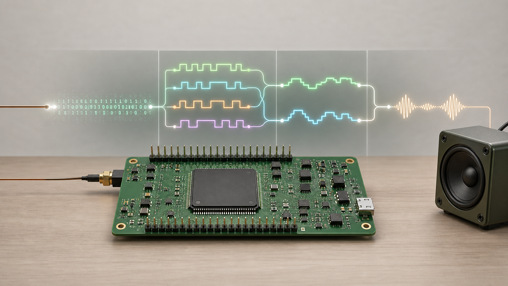
One Pin Works In Both Directions
The companion One-Pin Quadrature/SDM RF Transmitter crosses the reverse boundary. Two one-bit control streams select four carrier phases, gate one iCE40 output pin, and drive a resonant network.
An RTL-SDR Blog V4 received that transmitter through the 8.5 kΩ-coupled resonant tank and placed it beside a live PTC channel in CubicSDR. The transmitter and receiver form complementary explorations of the same question: how much RF behavior can one FPGA pin carry?
The Receiver Moves The Oscillator Inside The FPGA
A conventional receiver amplifies weak RF, multiplies it against a strong local oscillator, produces IF or baseband, digitizes amplitude, and then recovers audio. That proven architecture also creates an RF containment problem: the oscillator can leak, radiate, and couple across the board.
The ADC asks the analog front end to preserve clean amplitude and provide enough drive. Later stages add sine and cosine tables, multipliers, trigonometric mixing, and often atan2 phase extraction.
This receiver hides the local-oscillator action inside the FPGA and preserves crossing time instead of multi-bit RF amplitude.
RF crosses a threshold; digital logic carries the rest.
Threshold Crossings Replace Amplitude Samples
The FPGA input compares incoming RF with its midpoint. Each crossing produces a zero or one: no multi-bit sample word and no explicit amplitude at the pin.
An ideal fixed midpoint obeys sign(A cos(ωt)) = sign(cos(ωt)) for every A > 0. Two clean sinusoids that differ only in amplitude therefore produce the same transition stream.
Crossing time still carries phase and frequency structure. FM places its information in changing instantaneous frequency, which makes that representation especially direct. Known noise or dither, threshold offset, hysteresis, or a swept threshold can also break the scale ambiguity for a calibrated detector; calibrated front-end gain can then refer the result to the RF input plane.
RF in, transition stream out.
That choice removes most of the inherited analog and arithmetic machinery in one stroke.
Neural Circuit Search Supplied The Key Insight
About eighteen months earlier, neural-network training explored digital circuit layouts on multiplexer fabrics through backpropagation. A 50-50 binary noise process at the weight generator made simple circuits, including adders, far more trainable despite digital logic's sharp nonlinearities.
That work supplied a durable lesson:
information can survive as binary stochastic structure.
Sigma-delta ADC and DAC waveforms reinforced the idea from another direction: a smooth analog signal can inhabit a digital pulse stream. Transitions can carry more structure than a sampled-amplitude model suggests.
A sigma-delta RF front end would feed its digital output back into the analog side and move the threshold dynamically, recreating strong pulsing activity at the receiver boundary. The final design retained the information insight and used a quiet fixed threshold.
the one-pin input carries a rich field of transitions.
The Pin Preserves Phase And Frequency Structure
The fixed threshold converts RF amplitude into crossings and carries enough phase and frequency structure to recover intelligible FM audio.
In a noise-dominated region, coherent statistics of the one-bit stream vary with signal-to-noise ratio. A calibrated input gain, threshold, and noise reference—or a measurement mode that sweeps the threshold—can turn those statistics into signal-presence and relative-strength measurements at the RF input plane.
The present receiver uses crossing structure for demodulation. The next measurement plane can add absolute volts or dBm and a conducted transmitter-to-receiver loop while keeping the one-bit signal path intact.
DDR Samples Become I/Q Bit Lanes
The selected fm_radio_nov15.sv design clocks one iCE40 DDR input primitive with the source-labeled 168 MHz sampler clock and records two threshold decisions per cycle. Logic shifts the even and odd decisions into history, then applies fixed ordering and inversion patterns to construct two 16-lane words named samples_i and samples_q.
The source defines a 270-degree clock signal while the instantiated input path uses the single DDR sampler. Lane patterns reorganize that decision stream into its quadrature structure.
The downstream logic receives:
- direct and quadrature bit lanes,
- a compact input representation for DDS-controlled one-bit mixing,
- and a Weaver-style recombination path intended to reject the image.
Earlier notebook pages trace the route to this architecture; the November 15 source fixes the parameters for the implementation shown here.
Weaver Recombination Cancels The Image
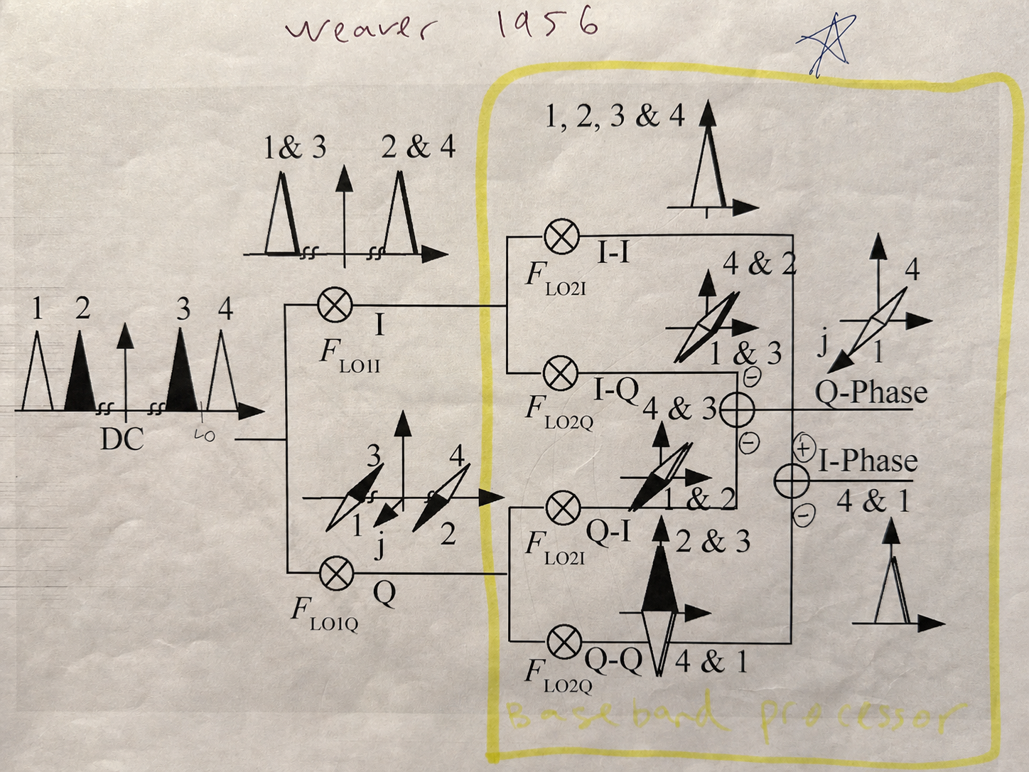
Weaver's method translates quadrature paths twice and recombines four products so the wanted sideband adds while the image cancels. The selected receiver source has the same structural idea at one-bit resolution: I and Q lane patterns, two intended-quadrature DDS sign bits, four XOR-and-popcount product terms, and sum/difference recombination.
The RTL translates Weaver's recombination principle into a one-bit digital datapath while using its own threshold sampler, accumulators, and FM discriminator.
XOR Gates Perform The Quadrature Mixing
Thresholded quadrature streams reduce mixing to controlled inversion. DDS sign bits drive XOR operations across the one-bit lanes, and population counts turn those products into signed baseband contributions.
The entire digital mixer therefore uses logic instead of sine tables, cosine tables, and amplitude multipliers.
The XOR-gate detector offers adjacent context: XOR duty cycle can encode phase difference in one-bit topologies. In this receiver, XOR performs the mixers and the later I/Q cross product performs FM recovery.
DDS Tuning Without a Sine Table
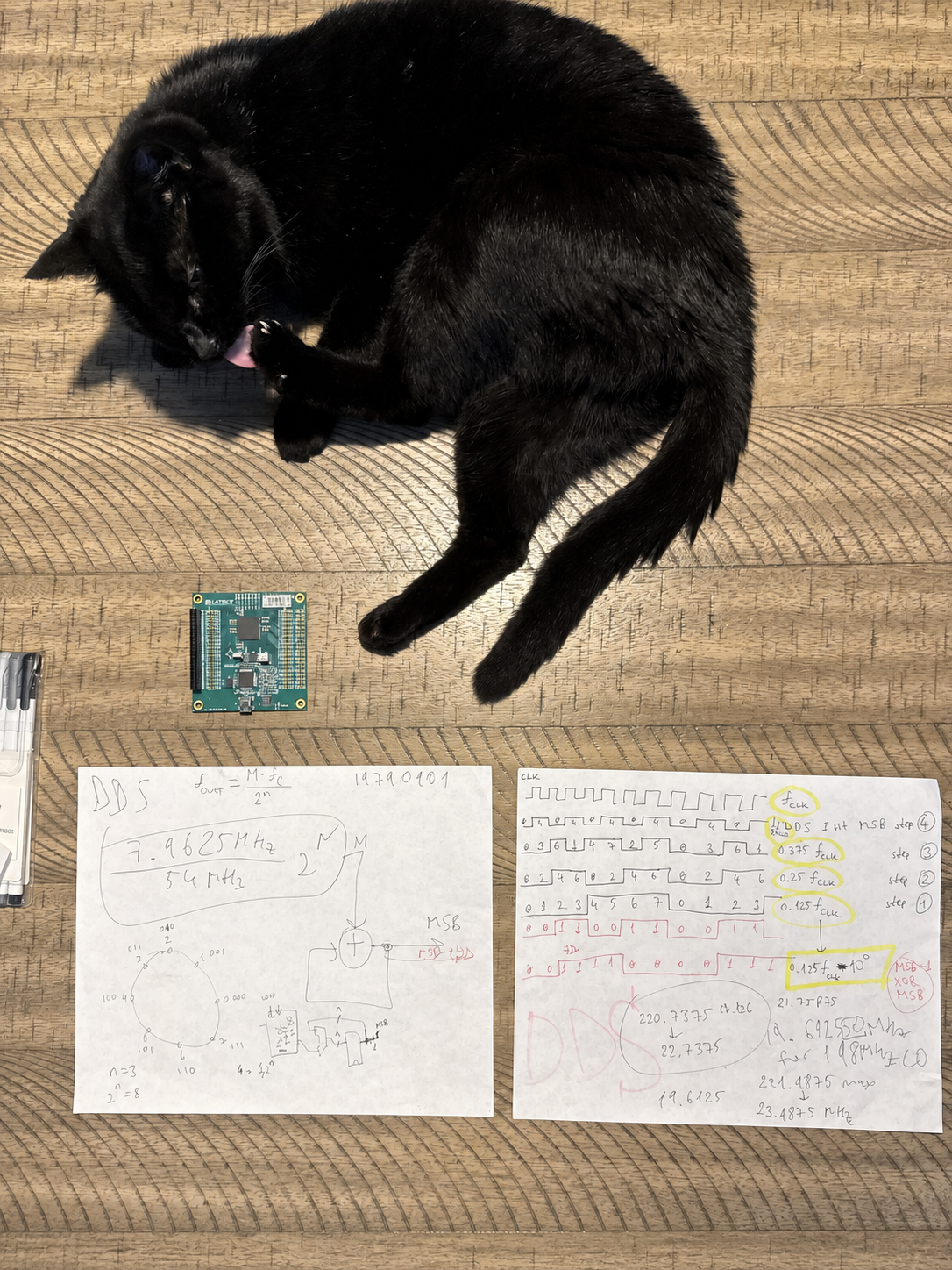
A direct digital synthesizer adds a tuning word to a phase accumulator every clock. For an N-bit accumulator, the basic relationship is fout = M fclock / 2N. A full DDS can map phase into sine and cosine amplitude. This receiver takes the shorter implementation path: it consumes the accumulator sign or most-significant bit as a square-wave, one-bit LO.
The source contains one 49-bit tuning path and a second accumulator intended to stay in quadrature. Their sign bits control the XOR mixers. Analog Devices MT-085, Fundamentals of Direct Digital Synthesis explains the phase-accumulator model, tuning resolution, aliasing, and spurs. AMD's DDS Compiler core overview covers quadrature synthesizers for FPGA digital downconverters. The iCE40 source implements its own sign-bit path.
A Cross Product Recovers FM Directly
Many FM demodulators recover absolute phase with atan2 and then differentiate it. Earlier DQPSK work suggested a shorter path: measure relative rotation between successive I/Q vectors directly.
The post-accumulator baseband therefore feeds this geometric relation:
Xn = In-1Qn - Qn-1In = |zn||zn-1| sin(φn - φn-1)
The expression computes the 2D cross product of successive I/Q vectors in the operand order used by the source. Reversing the operands changes only output polarity.
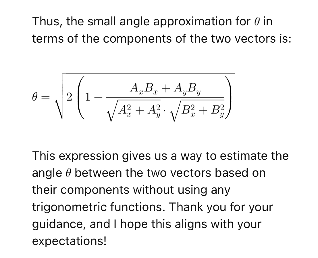
For small phase steps, the result gives a magnitude-weighted sine of relative rotation. FM turns that rotation into audio with two multiplications and one subtraction.
A centered CW produces approximately zero phase step and cross product. An offset CW appears approximately as DC, while FM produces a changing output. A parallel energy and coherence path can add calibrated signal classification without changing the audio discriminator.
Eight Operations Carry RF To Audio
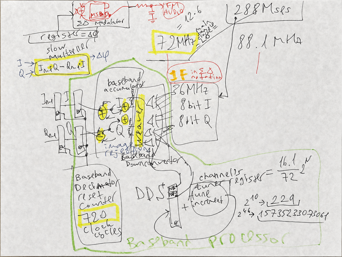
The baseband accumulators accept 80 updates of the 21 MHz processing clock, then use one cycle to transfer and reset. This rectangular integrate-and-dump stage performs the rate change before cross-product demodulation and sigma-delta audio output.
The complete chain follows eight direct operations:
- one logical differential FPGA input site receives RF,
- the input threshold converts RF into a binary transition stream,
- fixed lane patterns reorganize DDR decisions into 16-lane I/Q words,
- DDS sign bits control four XOR-and-popcount product terms,
- Weaver-style sum/difference recombination translates the selected channel,
- 80 processing-clock updates integrate before one transfer/reset cycle,
- a cross product between successive I/Q vectors recovers FM phase movement,
- and a sigma-delta output stage produces sound.
One thresholded RF stream enters; one audible pulse stream leaves.
The Verilog Shows Every Stage
New to this build vocabulary? Follow the FPGA and Verilog course through modules, constraints, Yosys, nextpnr, IceStorm, and bitstreams, then return to this receiver's unusual RF signal path.
one-pin-RF/README.md maps the source tree. fm_radio_demo_2026/fm_radio_nov15.sv contains the receiver described here, and build.sh selects it for an iCE40 UP5K build. The nearby fm_radio_2026_pin_4_3.sv supplies a near-identical retuned variant.
The build path sends SystemVerilog through Yosys, targets UP5K SG48 in nextpnr with the pin constraints, packs the bitstream through IceStorm, and downloads it through dfu-util. The archived November 15 file uses the identifier n in both sample-shift ranges; define that lane-history width before running this source snapshot.
read_verilog -sv ./fm_radio_nov15.sv
synth_ice40 -top top -json ./build/fm_radio.json
nextpnr-ice40 --ignore-loops --pre-pack ./timing.py --freq 336 --up5k --package sg48
icepack ./build/fm_radio.txt ./build/fm_radio.bin
The relevant pin boundary is one RF input and one sigma-delta audio output. The constraint file maps DIFF_PINS_4P_3N to package pin 4 and PIN2 to package pin 2.
input DIFF_PINS_4P_3N,
output PIN2,

wire [1:0] RF4X_SAMPLES;

SB_IO #(
    .PIN_TYPE(6'b000000),
    .IO_STANDARD("SB_LVDS_INPUT")
) ddr_sampler_2 (
    .PACKAGE_PIN(DIFF_PINS_4P_3N),
    .INPUT_CLK(CLK_168_MHZ),
    .D_IN_0(RF4X_SAMPLES[0]),
    .D_IN_1(RF4X_SAMPLES[1])
);
The source calls the DDR input the heart of the radio. It samples binary RF decisions on both clock edges, then folds even and odd history into two 16-bit quadrature words through fixed ordering and inversion.
samples_even <= {samples_even[n-1:0], RF4X_SAMPLES[0]};
samples_odd  <= {samples_odd [n-1:0], RF4X_SAMPLES[1]};

samples_i <= {
  samples_even[7],  samples_odd[7],
 ~samples_even[6], ~samples_odd[6],
  samples_even[5],  samples_odd[5],
  // same alternating pattern continues through bit 0
};

samples_q <= {
 ~samples_even[7],  samples_odd[7],
  samples_even[6], ~samples_odd[6],
 ~samples_even[5],  samples_odd[5],
  // same quadrature pattern continues through bit 0
};
Controlled inversion performs the digital mixing. Four repeated accumulation blocks XOR one-bit I/Q lanes against the two DDS sign bits, population-count each product, and recombine the terms into the baseband accumulators.
sum <=
    { 4'd0, samples_i[ 0] ^ dds_ch1[CH1_MSB] }
  + { 4'd0, samples_i[ 1] ^ dds_ch1[CH1_MSB] }
  + { 4'd0, samples_i[ 2] ^ dds_ch1[CH1_MSB] };

sum_qq <=
    { 4'd0, samples_q[ 0] ^ dds_ch1_90[CH1_MSB] }
  + { 4'd0, samples_q[ 1] ^ dds_ch1_90[CH1_MSB] }
  + { 4'd0, samples_q[ 2] ^ dds_ch1_90[CH1_MSB] };
The FM stage multiplies current and previous baseband I/Q values in cross-product form, then feeds the result into the sigma-delta output. A future parallel path can derive I/Q energy and coherent-carrier statistics from the same baseband words.
phase_delta <= decimator[DECIMATOR_MSB] ? (
  samples_bb[25:10] * samples_q_bb[25:10]
  -
  samples_bb_q[25:10] * samples[25:10]
) : phase_delta;

sd_dac <= {2'd0, phase_delta, 16'd0} + 34'd6442450944 +
  (dac_out ? 34'd8589934592 : 34'd8589934591);

dac_out <= sd_dac[SD_DAC_MSB];
assign PIN2 = ~dac_out;
The Verilog connects the whole receiver: thresholded RF enters one logical differential input, the iCE40 DDR primitive samples it, lane patterns build I/Q, DDS sign bits control one-bit mixers, the cross product recovers FM, and sigma-delta output produces the audio bitstream.
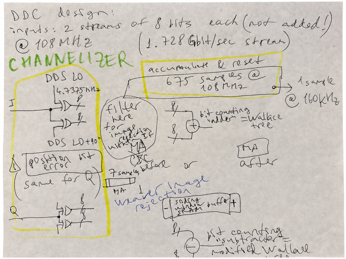
Three Notebook Designs Trace The Receiver's Evolution
The notebook moves from an early sampling plan through a 108 MHz channelizer to a multi-channel receiver architecture. The November 15 source implements the final single-channel path described above.
dirty_ptc_nov3.sv.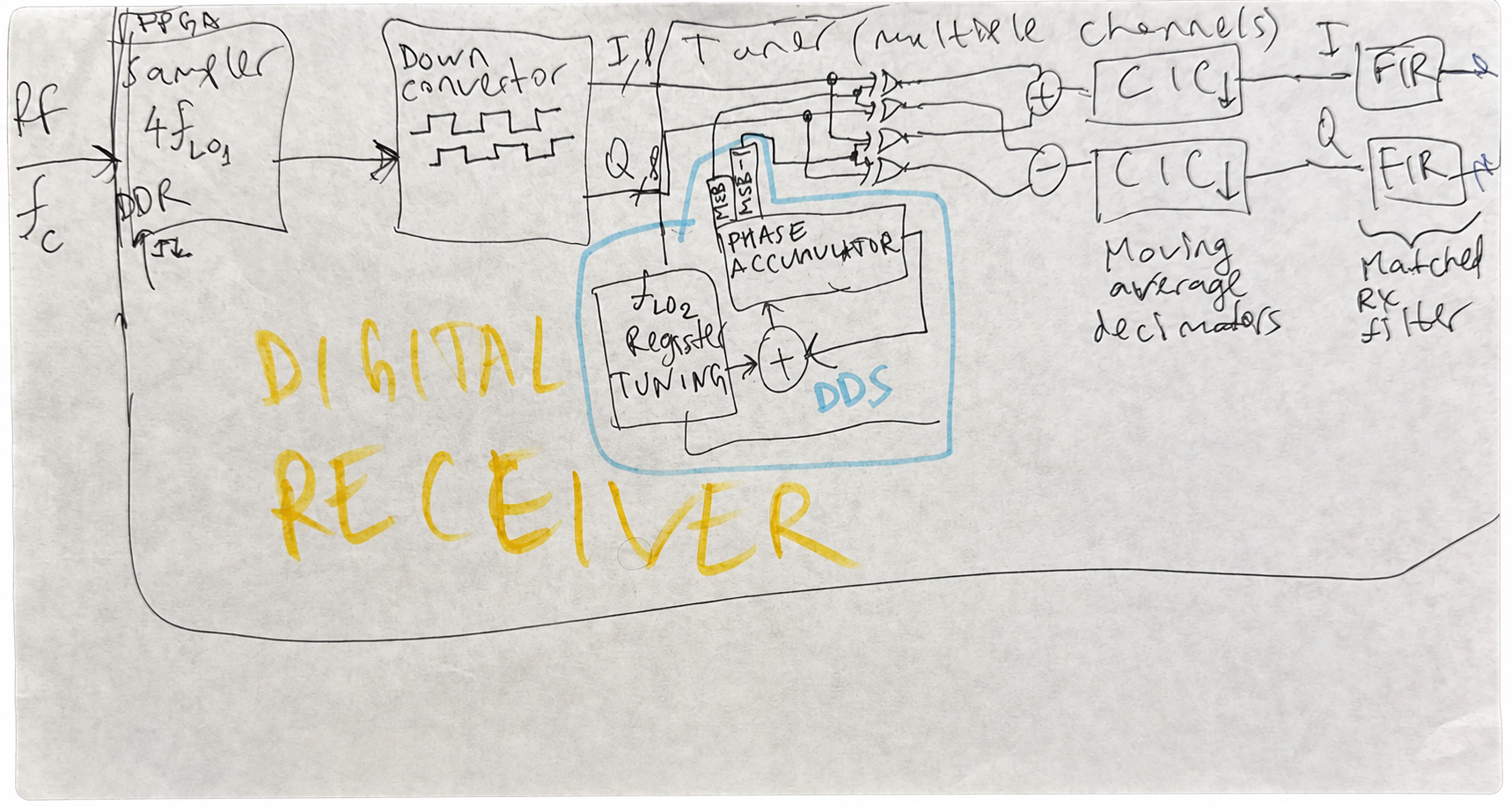
The 80-Sample Window Sets The Channel Shape
The 21 MHz processing clock performs 80 accumulator updates, then spends one clock transferring and resetting the accumulator. This produces an I/Q update rate of 21 MHz / 81 = 259.26 kS/s.
For that 80-update rectangular window alone, the calculated digital response is:
- one-sided −3 dB frequency: approximately 116 kHz
- first null: 262.5 kHz
- response at 200 kHz offset: approximately −10.9 dB
- first sidelobe: approximately −13.3 dB
The 259.26 kS/s output has a 129.63 kHz Nyquist frequency, where the rectangular window is already approximately −3.82 dB. Responses outside that range alias into the output, so aliases are part of the receiver measurement, not a detail to omit.
These values come directly from the rectangular-window calculation. Because thresholding precedes the digital filter, a strong off-channel signal can dominate the crossing stream before channel selection. A two-tone test—holding the wanted signal near sensitivity while raising an adjacent signal—will measure blocker performance.
The RTL names the logical port DIFF_PINS_4P_3N and configures it as SB_LVDS_INPUT. That mode uses the pin-4/pin-3 differential comparator pair; Lattice documents automatic assignment of the complementary pin. Both the RF-bearing input and its reference or bias companion belong to the receiver boundary. For 2.5 V VCCIO, the iCE40 UltraPlus data sheet guarantees differential-input HIGH and LOW regions at +250 mV and −250 mV. A calibrated voltage and bias fixture on both pins can map that digital receiver boundary into absolute RF input power.
Six Conventional Blocks Disappear
The working FM path removes six blocks that conventional receivers treat as fundamental:
- no strong external local oscillator spraying into the board
- no Gilbert-cell-centered analog front end
- no fast amplitude-preserving ADC at RF or IF
- no sine/cosine lookup tables
- no sine/cosine multiplier chain
- no
atan2-based phase extractor
The receiver recovers audio after all six disappear. That result turns reduction into an engineering tool: the design reveals which machinery the signal actually needs.
The Receiver Changes The System Boundary
Thresholded RF enters one digital pin, and the FPGA recovers audio through timing, logic, and accumulated relative phase. That boundary opens a receiver architecture with dramatically less analog apparatus and a signal path that digital designers can inspect end to end.
An older Xilinx publication describes an FM receiver along related lines: quiet input biasing, direct threshold behavior, and no front-end sigma-delta feedback. The independent path confirms the architectural value of treating transitions as the RF representation.
The one-pin receiver answers the question that drove the build:
How much radio do you actually need?
Far less than the conventional signal chain suggests.
The Same Pin Can Become A Calibrated Detector
The FM path already recovers audio from threshold crossings. A parallel measurement plane can classify signals and report calibrated receiver performance:
From the same thresholded RF pin, distinguish no detected signal, CW, and modulated RF at a selected frequency, with stated bandwidth, sensitivity, probability of detection, false-alarm rate, and blocker rejection.
That requires a quiet capture path for signed post-filter I/Q, raw one-density, transition count, and discriminator output; a conducted and shielded 50 Ω fixture; a frozen detector rule; terminated-input calibration; CW power and frequency sweeps; two-tone blocker tests; and FM SINAD, distortion, and deviation-linearity measurements.
The resulting report can state: No signal of the tested class appeared within B Hz of f during T. At or above X dBm, the detector reached PD of at least 0.90 at PFA = Y per stated dwell and searched bin.
Can One Bit Tell What Is There? will carry those measurements and turn the same one-pin architecture into a quantified detector.