Teach Microelectronics in Maker Spaces
January 17, 2024
Microelectronics belongs in maker spaces. Children and adults should learn how active devices, lithography, deposition, etching, measurement, packaging, and circuit design work by building micrometer-scale chips and PCBs locally.
Brian Greenforest proposes that every American town grow semiconductor talent through direct physical practice.
Bring the Semiconductor Process Into Reach
A community laboratory can teach masks, photoresist, exposure, development, etching, deposition, oxidation, microscopy, probing, and failure analysis at geometries that visible equipment can handle.
Students can connect each process step with transistor behavior, digital logic, PCB interconnect, and the product that uses the circuit.
Grow Capability Instead of Importing Dependency
University research remains essential, and maker-space education can widen the path into that expertise. A larger domestic talent base strengthens manufacturing, repair, security, and invention across many industries.
Schools, towns, universities, equipment donors, and semiconductor professionals can build the curriculum and laboratory. Bring STEM home and let every community make active circuitry.
LinkedIn status when archived: Visible to anyone on or off LinkedIn.
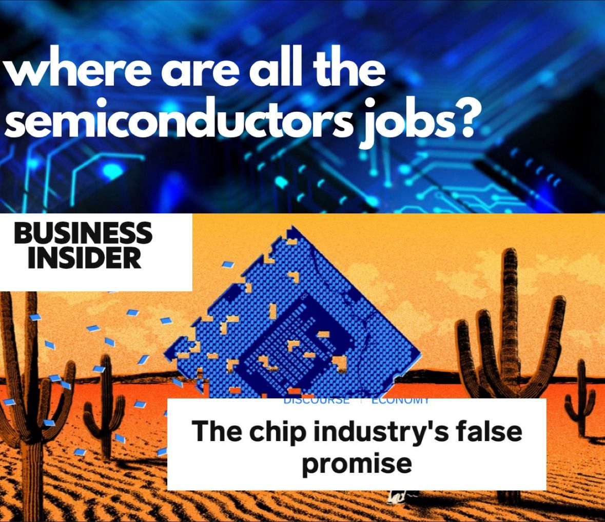
I am pretty sure chip industry is a PhD's business, not even blue collar's. EU could win this game in long run, with all the university support... What we need instead is to teach kids microelectronics at #maker spaces instead of how to use Chinese cheap but proprietary 3D printers. Bring #stem home. Make micrometer-process chips and PCBs at every small town in the United States of America. We need to raise talent, not import ad infinitum and hope security won't ever become way too compromised. Not just in chips. 🇺🇸